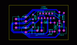
Here is the schematic for the LM3886 "XY Power Amp" circuit board that is widely available on Ebay:


I couldn't find the schematic posted anywhere, so I traced the routing myself.
These are very inexpensive - I just bought 10 bare boards for about US$25, with shipping included. I plan to build up a set of these amp boards using good quality components for use in active speaker projects. If you want moderate power levels (30W@8 ohms or 50W@4 ohms) and low distortion across the audio band, this is probably the simplest and least expensive way to get it.
-Charlie
Last edited:
RF attenuation is omitted.
Very easy to correct: add a parallel cap across R5 either on top of the PCB, or underneath the PCB.
Output Thiele Network is omitted.
Very easy to correct: remove the output terminal block. Connect the Zobel capacitor in the spare location.
Tap off the speaker output from the top end of R1.
The other half of the Thiele Network (L//R) can be mounted offboard in the line that joins the amp PCB to the speaker terminals fitted to the chassis.
The speaker return connects to the Main Audio Ground, not to the amp PCB.
Finally,
check to see how R5 and C4 are connected to Signal Ground. They must not connect to Power Ground on the underside of the PCB.
Last edited:
RF attenuation is omitted.
Very easy to correct: add a parallel cap across R5 either on top of the PCB, or underneath the PCB.
Output Thiele Network is omitted.
Very easy to correct: remove the output terminal block. Connect the Zobel capacitor in the spare location.
Tap off the speaker output from the top end of R1.
The other half of the Thiele Network (L//R) can be mounted offboard in the line that joins the amp PCB to the speaker terminals fitted to the chassis.
The speaker return connects to the Main Audio Ground, not to the amp PCB.
It was never quite clear to me why these "Thiele" (zobel?) networks were needed. Is this to shunt RF picked up by long speaker cable runs to ground?
Finally,
check to see how R5 and C4 are connected to Signal Ground. They must not connect to Power Ground on the underside of the PCB.
Yes, it is as shown on the schematic, with R5 and C4 connecting to the signal ground, which is isolated from the power ground.
-Charlie
Hi,
the Thiele Network is there to help with stability of the amplifier depending on what is connected to the chassis speaker terminals.
A Zobel on it's own does very little to attenuate RF and back emf coming from the speaker side of the chassis.
Thanks, Andrew. I did some reading on the web and found some nice explanations of each part of the output network.
But in my case, I will be directly connecting the chip amps to drivers with nothing but a short piece of wire in between. I found this old post by Svante about this scenario:
I would tend to agree with Svante - that none of the output network(s) are really needed. I don't see how the complex impedance of a single driver is going to matter all that much in this case. But I would like to get your opinion, too.If you use a normal solid state amplifier with no crossover between the amp and speaker, impedance compensation is not needed.
Impedance compensation can only be needed when the source (=amp+filter+cables) has an output impedance that is comparable with that of the driver.
Some say that a resistive load is better for the amplifier than a reactive load, but in normal cases, the load rather becomes more difficult for the amp if a compensating network is used even though it becomes resistive.
-Charlie
I was planning on buying one of these XY Power Amp kits from Ebay soon - So I'd be interested on what shortcomings it has (and how one can remedy them).
It will be used to drive a small pair of DIY bookshelf speakers.
Just follow AndrewT's suggestions to add on some extra networks at the input and output of the PCB.
Charlie
Just follow AndrewT's suggestions to add on some extra networks at the input and output of the PCB.
Charlie
I will, however unfortunately I have no idea what RF attenuation is and what value of cap to use...
Zobel/Thiele network? Purpose? Components involved?

Can you point me in the right direction please.
Thanks,
Chris
Hi AndrewT,
I've looked through the datasheet and see the optional components section however it doesn't mean much to me - nevermind the implementation thereof.
Is there anyway you could briefly tell me what to add and what each addition would do?
I would be grateful.
Kind Regards,
Chris
I've looked through the datasheet and see the optional components section however it doesn't mean much to me - nevermind the implementation thereof.
Is there anyway you could briefly tell me what to add and what each addition would do?
I would be grateful.
Kind Regards,
Chris
Hello CharlieLaub,
Have you finished your project of LM3886 ? Does it produce good sound ?
I also want to build a Lm3886 power amp same as you. But I have few question regarding LM3886.
Do you add the speaker protection board between speaker and your LM3886 output ?
Do you add pre-amp board (NE5532 op-amp) infront of LM3886 input?
I searched some of forum or ebay, most of them also connect speaker protection board and pre-amp board for LM3886.
What is your comment ?
Regards
hpq
Hi guys,
Thanks for all inputs.
Regarding the optional components actually I want to makes a prototype based upon the schematic in the datasheet and then I will improve it and add the optional components just if needed.
I have made the circuit directly based upon the schematic in the datsheet before (all components were connected to gather without any pcb) and it worked fine for me.
Ok I tried to modify the PCB as you noted. Plz kindly take a look at the new pcb and let me know your ideas.
Thanks a bunch
Attachments
Andrew,
Thanks a bunch for your reply,
Sorry What do you mean by that plz? PIN9 is completely seperated from PIN10 so what do you mean by loop area here?
What is interference upsetting?
Yet I do not know what do you mean by loop area here so I do not know how to solve the problem.
Thanks
Thanks a bunch for your reply,
The loop area for PIN9 to PIN10 is enormous.
Sorry What do you mean by that plz? PIN9 is completely seperated from PIN10 so what do you mean by loop area here?
Expect trouble due to interference upsetting the unstabilised amplifier.
What is interference upsetting?
The loop area for PINs 4 & 5 via the two decoupling caps is even more enormous.
Yet I do not know what do you mean by loop area here so I do not know how to solve the problem.
Thanks
Last edited:
Are you aware that an aerial that picks up interference is a loop?
Now start at PIN9 and follow the traces and components: to R701, to R702, through R702, to C555, through C555, to star ground, to Input PIN1, to PIN2, to R700, through R700, to PIN10.
Now shade in the area enclosed within that route.
That is your loop area. That is your aerial picking up interference.
You must make that group of components and traces and pins as small and as compact as possible and try to minimise the loop area.
Repeat for the output.
Repeat for the Zobel.
Repeat for the PSU rails.
Hi Epilot.
Could you upload the pcb file to the forum. it would be a lot easier to modifiy the pcb and show you that way.. ps what pcb software are you using..
Regards Ian
Hi sir,
I am using the Proteus software to design the PCB's. If you have the software then just let me know so that I put the PCB file here.
- Status
- This old topic is closed. If you want to reopen this topic, contact a moderator using the "Report Post" button.
- Home
- Amplifiers
- Chip Amps
- LM3886 PCB