Hello,
I'd like some input on something I recently cooked up after studying many threads and projects here on DIYAUDIO and elsewhere online:
• I want to drive headphones fully balanced.
• I don't want too many components in the signal path.
• I'd like to use ICs throughout.
• I need to incorporate volume control.
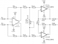
I came up with the attached schematic (general building block, single channel).
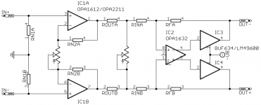
It involves a balanced input stage/buffer using an OPA1632 (IC1) in a conventional topology (see datasheet), possibly contributing some gain.
Followed by a differential attenuator (R14/R15/P1) in a shunt configuration, damping both noninverting and inverting phase in a fully balanced manner (i.e. using only a single gang/pot and no ground reference).
Last is a differential output stage featuring TPA1632A2 (IC11, see datasheet), using both amplifiers tied to a common virtual ground.
A couple problems I foresee:
• In this configuration IC1 would be required to drive the voltage divider(s) around the shunting volume pot. In order to achieve full attenuation the impedance level would have to be rather low.
That's why I mentioned that IC1 could contribute some gain. I could also live with an instrumentation amp incorporating two additional opamps in front of IC1. I'm not certain!
• The voltage divider consisting of R14/P1 and R15/P1 (respectively) could be limited in it's attenuation range. Increasing it's impedance level would introduce unnecessary noise into the circuit. I'm not sure!
• The ouptut stage design circumvents the more obvious bridge topology, thus ensuring balanced impedances on all respective nodes. It dosn't feature "super symmetry", though, so it could waste some potential that the OPA1632 enables. I just don't know!
What do you think?
Thanks,
Sebastian.
I'd like some input on something I recently cooked up after studying many threads and projects here on DIYAUDIO and elsewhere online:
• I want to drive headphones fully balanced.
• I don't want too many components in the signal path.
• I'd like to use ICs throughout.
• I need to incorporate volume control.
I came up with the attached schematic (general building block, single channel).
It involves a balanced input stage/buffer using an OPA1632 (IC1) in a conventional topology (see datasheet), possibly contributing some gain.
Followed by a differential attenuator (R14/R15/P1) in a shunt configuration, damping both noninverting and inverting phase in a fully balanced manner (i.e. using only a single gang/pot and no ground reference).
Last is a differential output stage featuring TPA1632A2 (IC11, see datasheet), using both amplifiers tied to a common virtual ground.
A couple problems I foresee:
• In this configuration IC1 would be required to drive the voltage divider(s) around the shunting volume pot. In order to achieve full attenuation the impedance level would have to be rather low.
That's why I mentioned that IC1 could contribute some gain. I could also live with an instrumentation amp incorporating two additional opamps in front of IC1. I'm not certain!
• The voltage divider consisting of R14/P1 and R15/P1 (respectively) could be limited in it's attenuation range. Increasing it's impedance level would introduce unnecessary noise into the circuit. I'm not sure!
• The ouptut stage design circumvents the more obvious bridge topology, thus ensuring balanced impedances on all respective nodes. It dosn't feature "super symmetry", though, so it could waste some potential that the OPA1632 enables. I just don't know!
What do you think?
Thanks,
Sebastian.
Attachments
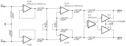
Well, I finally got around to trying an early prototype variant. I modified the circuit by introducing an instrumentation amp stage in front of the balanced opamp, which gives me a high impedance, fully differential gain stage (independent of source impedances and source grounding scheme), still with single-pot volume control.
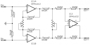
The first picture shows the circuit I tried, it leaves out the buffers as they are not required in order to try the concept of a single pot volume control in front of the OPA1632. Besides, I decided to use different buffers than the TPA6102A2/THS6012 that I earlier proposed, as I became aware of difficulties with this current feedback amplifiers' stability into low impedance loads.
The second picture shows my prototype with a dual opamp (wired as instrumentation stage) on the left with a pot for gain adjustment (input gain setting allows for different sensitivities of different headphones). On the right is an OPA1632 with a gain of 1. In the middle there's the differential voltage divider with two 1kOhm series resistors and a 25kOhm potentiometer.
I got inspired during a discussion about The Wire and it's lack of volume control in the design scope (my personal opinion).
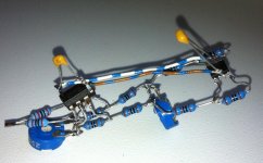
No kidding, the build shown below works like a charm, even stable (as long as the cheap pots still have contact") ). Speed is an issue, though. My first tests were with an OPA1612 (equivalent to OPA2211) in the instrumentation stage, but I didn't manage to get the circuit ringing free under all circumstances due to sloppy wiring, decoupling and grounding. While improving on the flaws, some of the IC's SMD legs gave up and broke off. So I had to continue with the only DIL dual-opamp I had in stock: an RC4558...
). Speed is an issue, though. My first tests were with an OPA1612 (equivalent to OPA2211) in the instrumentation stage, but I didn't manage to get the circuit ringing free under all circumstances due to sloppy wiring, decoupling and grounding. While improving on the flaws, some of the IC's SMD legs gave up and broke off. So I had to continue with the only DIL dual-opamp I had in stock: an RC4558...
The first picture shows the circuit I tried, it leaves out the buffers as they are not required in order to try the concept of a single pot volume control in front of the OPA1632. Besides, I decided to use different buffers than the TPA6102A2/THS6012 that I earlier proposed, as I became aware of difficulties with this current feedback amplifiers' stability into low impedance loads.
The second picture shows my prototype with a dual opamp (wired as instrumentation stage) on the left with a pot for gain adjustment (input gain setting allows for different sensitivities of different headphones). On the right is an OPA1632 with a gain of 1. In the middle there's the differential voltage divider with two 1kOhm series resistors and a 25kOhm potentiometer.
I got inspired during a discussion about The Wire and it's lack of volume control in the design scope (my personal opinion).
No kidding, the build shown below works like a charm, even stable (as long as the cheap pots still have contact
). Speed is an issue, though. My first tests were with an OPA1612 (equivalent to OPA2211) in the instrumentation stage, but I didn't manage to get the circuit ringing free under all circumstances due to sloppy wiring, decoupling and grounding. While improving on the flaws, some of the IC's SMD legs gave up and broke off. So I had to continue with the only DIL dual-opamp I had in stock: an RC4558... Attachments
Last edited:
A couple problems I foresee:
• In this configuration IC1 would be required to drive the voltage divider(s) around the shunting volume pot. In order to achieve full attenuation the impedance level would have to be rather low.
That's why I mentioned that IC1 could contribute some gain. I could also live with an instrumentation amp incorporating two additional opamps in front of IC1. I'm not certain!
Thanks,
Sebastian.
I can't see any reason why the first circuit wouldn't work fine. If your two series resistors in the volume circuit are both 1k, then even with the pot shorted, the opa1632 still sees a 2K ohm load at absolute minimum, which should be no problem at all.
I can't see any reason why the first circuit wouldn't work fine. If your two series resistors in the volume circuit are both 1k, then even with the pot shorted, the opa1632 still sees a 2K ohm load at absolute minimum, which should be no problem at all.
Thanks for the reply.
I agree that the OPA1632 is never exposed to a short or any ill defined output load. What I was worried about, though, was the overall gain/transfer function possibly being influenced by the highly varying voltage divider impedance. But as the output stage has it's amplifiers in noninverting mode, I now see that the output stage gain doesn't depend on it's input impedance. Bingo.
Although, the same approach is applied in the current circuit. But as the voltage divider is now in front of the fully differential opamp (where gain setting depends on the ratio between feedback impedance and source impedance), there might be an influence of the pot on the OPA1632's gain.
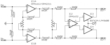
The reason why I'm putting the pot inbetween instrumentation stage and differential amp is because I now want to drive (diamond) buffers in the output. They can be connected without output damping resistors, thus enabling the lowest output impedance (see attachment below). As the instrumentation stage can be built with or without providing gain, I've shown a gain potentiometer - which could be left out if so desired.
I don't yet see it: do I have to worry about the volume control adversely affecting the behaviour of the OPA1632 and it's gain setting? The way I see it, the gain setting around the OPA1632 (which is essentially that of two inverting opamps) would have to account for the source impedance including the voltage divider - which varies.
Thanks,
Sebastian.
Attachments
The gain will be affected because the input impedance changes. But whether that is a problem depends on the values you're using. Remember that best case, the differential input impedance will be 0, and worst case it will be 2k ohms in parallel with the volume pot, (if you're still using 1K resistors on the volume circuit).
So yeah, it can screw up the gain a bit. But unless your input resistors to the opa1632 are very small (do you have the fda wired for a lot of gain?), this effect is going to be completely swamped by the actual volume adjustments you're making. Gain will be highest when volume is muted, and lowest when volume is at maximum. So accept that your volume steps are going to be slightly smaller than specified if using a stepped attenuator, or if using a pot don't worry about it at all!
So yeah, it can screw up the gain a bit. But unless your input resistors to the opa1632 are very small (do you have the fda wired for a lot of gain?), this effect is going to be completely swamped by the actual volume adjustments you're making. Gain will be highest when volume is muted, and lowest when volume is at maximum. So accept that your volume steps are going to be slightly smaller than specified if using a stepped attenuator, or if using a pot don't worry about it at all!
Again, thanks for looking at it?
I'm afraid I need some clarification to wrap my head around all this, because I think it's not that easy...
Let's look at it in a split way first, perceiving each differential half of the fda. If attached a schematic with renamed components.
In case of an open input and no dedicated source resistors, the input impedance in front of each input varies between 0 (pot. at min.) and 1/2*Rpot (pot. at max.). With equal series resistors Rin on each input, it varies between Rin (pot. at min.) and 1/2*Rpot+Rin (pot. at max.).
As only the ratios account for the gain setting, let's consider a 1:10 divider ratio of series resistors and pot (i.e. 1k Rin, 20k Rpot) and a 1:1 ratio of the feedback resistor(s) Rf and Rin (i.e. 1k Rf).
With gain being set by the ratio Rf/Rg and Rg being the effective impedance seen from each input, we'll now have to look at a parallel value formed from the input resistor and half of the momentarily volume pot value: Rg=Rin||(1/2*Rvol)
With A=Rf/Rg, this would resolve to: A = Rf/(Rin||(1/2*Rvol)) = (Rf*1/2*Rvol)/Rin (right?)
I plan to have the fda at a gain of one (for best noise performance) or two (for makeup gain), not decided yet. Not higher.
In the above derivation, the gain in case of an open input was modeled.
What's with the buffer stage in front of it? This one shall be connected permanently, so the case of an open input would never occur in reality.
The buffer stage probably shouldn't work into the pot directly, as there's no point in exposing an opamp to a short without reason. So there would be a series resistance Rout in front of the pot (as depicted in my above schematic).
The calculations for such a network are given i.e. in chapter 11 (p. 15) in TI's Fully Differential Amplifiers application note (termination of input source, influence on gain).
What's with the output impedance of the buffer stage? Can this be incorporated in order to reduce the influence of the pot on the Rf/Rg variation? Can a purposely low Rout be used for good in this application? That's what I can't wrap my mind around yet.
Any help is appreciated!
Cheers,
Sebastian.
Remember that best case, the differential input impedance will be 0, and worst case it will be 2k ohms in parallel with the volume pot, (if you're still using 1K resistors on the volume circuit).
I'm afraid I need some clarification to wrap my head around all this, because I think it's not that easy...
Let's look at it in a split way first, perceiving each differential half of the fda. If attached a schematic with renamed components.
In case of an open input and no dedicated source resistors, the input impedance in front of each input varies between 0 (pot. at min.) and 1/2*Rpot (pot. at max.). With equal series resistors Rin on each input, it varies between Rin (pot. at min.) and 1/2*Rpot+Rin (pot. at max.).
As only the ratios account for the gain setting, let's consider a 1:10 divider ratio of series resistors and pot (i.e. 1k Rin, 20k Rpot) and a 1:1 ratio of the feedback resistor(s) Rf and Rin (i.e. 1k Rf).
With gain being set by the ratio Rf/Rg and Rg being the effective impedance seen from each input, we'll now have to look at a parallel value formed from the input resistor and half of the momentarily volume pot value: Rg=Rin||(1/2*Rvol)
With A=Rf/Rg, this would resolve to: A = Rf/(Rin||(1/2*Rvol)) = (Rf*1/2*Rvol)/Rin (right?
)So yeah, it can screw up the gain a bit. But unless your input resistors to the opa1632 are very small (do you have the fda wired for a lot of gain?), this effect is going to be completely swamped by the actual volume adjustments you're making.
I plan to have the fda at a gain of one (for best noise performance) or two (for makeup gain), not decided yet. Not higher.
In the above derivation, the gain in case of an open input was modeled.
What's with the buffer stage in front of it? This one shall be connected permanently, so the case of an open input would never occur in reality.
The buffer stage probably shouldn't work into the pot directly, as there's no point in exposing an opamp to a short without reason. So there would be a series resistance Rout in front of the pot (as depicted in my above schematic).
The calculations for such a network are given i.e. in chapter 11 (p. 15) in TI's Fully Differential Amplifiers application note (termination of input source, influence on gain).
Gain will be highest when volume is muted, and lowest when volume is at maximum. So accept that your volume steps are going to be slightly smaller than specified if using a stepped attenuator, or if using a pot don't worry about it at all!
What's with the output impedance of the buffer stage? Can this be incorporated in order to reduce the influence of the pot on the Rf/Rg variation? Can a purposely low Rout be used for good in this application? That's what I can't wrap my mind around yet.
Any help is appreciated!
Cheers,
Sebastian.
Attachments
In case of an open input and no dedicated source resistors, the input impedance in front of each input varies between 0 (pot. at min.) and 1/2*Rpot (pot. at max.). With equal series resistors Rin on each input, it varies between Rin (pot. at min.) and 1/2*Rpot+Rin (pot. at max.).
The buffer stage probably shouldn't work into the pot directly, as there's no point in exposing an opamp to a short without reason. So there would be a series resistance Rout in front of the pot (as depicted in my above schematic).
Cheers,
Sebastian.
No, when the pot is at minimum,the differential input impedance is equal to zero, or whatever very low value the pot goes to (a couple ohms). You don't want to look at each half separately as that will trip you up. So the minimum input impedance seen is 0, and the maximum is 2x Rin, since the output impedance of the buffer stage is very low, the two Rin resistors both go to a low impedance, so they appear in series. Since you're wiring the fda for fairly low gain, the feedback network resistors will be a bit larger (say maybe 10K ohms each) and the effect of the input impedance will be small.
The toughest load ever seen by the buffer is when the volume pot is at zero, but you still have the Rin resistors in series, so each buffer ic sees half of 2xRin, or just Rin. So if your input opamps are happy driving a load of Rin (check the datasheet for max current or sometimes they just say min load resistance) then you're fine.
are you connecting to a fixed impedance source - the 1632 gain changes with any added impedance from the source
typically this sort of dual inverting gain balanced inputs require high input Z noninverting buffers on the inputs to interface with a range of different sources
I have a CD player with > 1 K Ohm output Z due to the muting circuit - and other sources with <100 Ohms series R
once you have added the noniverting buffers you might as well put higher Z volume pots at the input as usually used in the majority of amps
are you connecting to a fixed impedance source - the 1632 gain changes with any added impedance from the source
typically this sort of dual inverting gain balanced inputs require high input Z noninverting buffers on the inputs to interface with a range of different sources
I have a CD player with > 1 K Ohm output Z due to the muting circuit - and other sources with <100 Ohms series R
once you have added the noniverting buffers you might as well put higher Z volume pots at the input as usually used in the majority of amps
Yeah he's buffering the opa & volume control. The problem with putting the volume control out front is that either you have to use four single-ended volume pots for real balanced input, or if you use a differential volume control as he is here, it then becomes dependent on the impedance of the source.
The circuit as shown is totally fine, just if you use a stepped attenuator the gain values won't be perfect. If you are using a pot it makes no difference whatsoever. As long as the network resistors on the fda are relatively large compared to the Rin resistors for the volume network, the change in gain should not be a problem.
Guys,
thanks for the feedback.
So basically the difference between instrumentation amplifier without pot and my circuit is that the source impedances in an INA are not common to both differential inputs of the FDA, whereas the FDA inputs in my circuit now have a common reference which they wouldn't have without the pot?
If that is true, I'd like to learn more about how noise performance of the FDA is affected. Considering the circuit with the pot, I figure that with the raised gain at high attenuation (low volume setting) noise increases considerably (and thus THD+N at low volumes is worsened).
Might it be better to enclose the voltage divider inbetween two differential buffers (i.e. make the core building block an INA again and move the pot and another differential buffer in front of it)?
Maybe, maybe not. I'd say it depends on whether you look at common mode or at differential mode properties. But I understand that a FDA is not a pair of single opamps.
Wouldn't that forbid a pot in that position, as the gain value a=Rf/Rin would have Rin approach zero with the pot value approaching zero?
Isn't this only true for either FDA gains a>>1 or at high impedance levels, both considerably contributing to output noise?
I originally thought that a strength of this approach could be to leverage on the excellent specs of the ICs at low gain and low impedance level...
Buffer stage opamps can be chosen accordingly in order to be specified into 1kOhm (i.e. those shown in the schematic are)
Assuming values like Rout=1k, Rin=10k and Rvol=20k, an overall gain of one and the 20k pot fully open, using the formulae on page 17 in the abovementioned TI application note I calculate Rf=12k.
I'm lost at deriving FDA local gain under the (most likely wrong) assumption that Rin approaches zero with the pot turned all the way down.
How would I derive the actual input impedance per input node for gain calculations?
Huh,
Sebastian.
thanks for the feedback.
No, when the pot is at minimum,the differential input impedance is equal to zero, or whatever very low value the pot goes to (a couple ohms).
So basically the difference between instrumentation amplifier without pot and my circuit is that the source impedances in an INA are not common to both differential inputs of the FDA, whereas the FDA inputs in my circuit now have a common reference which they wouldn't have without the pot?
If that is true, I'd like to learn more about how noise performance of the FDA is affected. Considering the circuit with the pot, I figure that with the raised gain at high attenuation (low volume setting) noise increases considerably (and thus THD+N at low volumes is worsened).
jcx said:typically this sort of dual inverting gain balanced inputs require high input Z noninverting buffers on the inputs to interface with a range of different sources
Might it be better to enclose the voltage divider inbetween two differential buffers (i.e. make the core building block an INA again and move the pot and another differential buffer in front of it)?
Rescue Toaster said:You don't want to look at each half separately as that will trip you up.
Maybe, maybe not. I'd say it depends on whether you look at common mode or at differential mode properties. But I understand that a FDA is not a pair of single opamps.
So the minimum input impedance seen is 0
Wouldn't that forbid a pot in that position, as the gain value a=Rf/Rin would have Rin approach zero with the pot value approaching zero?
So the minimum input impedance seen is 0, and the maximum is 2x Rin, since the output impedance of the buffer stage is very low, the two Rin resistors both go to a low impedance, so they appear in series. Since you're wiring the fda for fairly low gain, the feedback network resistors will be a bit larger (say maybe 10K ohms each) and the effect of the input impedance will be small.
Isn't this only true for either FDA gains a>>1 or at high impedance levels, both considerably contributing to output noise?
I originally thought that a strength of this approach could be to leverage on the excellent specs of the ICs at low gain and low impedance level...
The circuit as shown is totally fine, just if you use a stepped attenuator the gain values won't be perfect. If you are using a pot it makes no difference whatsoever. As long as the network resistors on the fda are relatively large compared to the Rin resistors for the volume network, the change in gain should not be a problem.
Buffer stage opamps can be chosen accordingly in order to be specified into 1kOhm (i.e. those shown in the schematic are)
Assuming values like Rout=1k, Rin=10k and Rvol=20k, an overall gain of one and the 20k pot fully open, using the formulae on page 17 in the abovementioned TI application note I calculate Rf=12k.
I'm lost at deriving FDA local gain under the (most likely wrong) assumption that Rin approaches zero with the pot turned all the way down.
How would I derive the actual input impedance per input node for gain calculations?
Huh,
Sebastian.
Last edited:
Well RIN is still equal to RFB assuming a gain of 1. When I say 'the input impedance is zero' I mean that the impedance of everything BEFORE RIN is zero. Imagine the two RIN's are connected together, which is obviously the case when the volume pot is turned all the way down.
Well RIN is still equal to RFB assuming a gain of 1.
I agree that this would lead to a local FDA gain of one, but seeing that the differential voltage divider presents an attenuator even at maximum pot resistance, the overall gain would be below one in case of Rf/Rin, no?
What am I missing? Am I wrong in assuming that the differential divider imposes an attenuation at full volume? I don't see it...
When I say 'the input impedance is zero' I mean that the impedance of everything BEFORE RIN is zero. Imagine the two RIN's are connected together, which is obviously the case when the volume pot is turned all the way down.
Woah, that's something entirely different than I took from your first description.
I totally agree that in front of the two Rin everything appears as zero with the pot turned down.
But that's not news, as this would be the case with a regular opamp and an unbalanced volume attenuator, too. Of course I assumed the pot to be shunting everything in front of Rin (and thus, in case of the differential circuit, connecting RinA and RinB) and the gain formula is still a=Rf/Rin.
Basically, when I'm looking at local FDA gain/feedback in the above circuit I have to account for the effective input impedance not being constant.
I now understand that in (the easier) case of the volume pot at zero the gain is simply Rf/Rin, whereas in case of the open pot the total effective input impedance seen by the FDA would resolve to
Rtot = Rin + (2Rout+Rpot)/2 (as explained in chapter 11 of the app note above).
Right?
Rtot = Rin + (2Rout+Rpot)/2 (as explained in chapter 11 of the app note above).
Right?
Input impedance in front of Rin should be (2*Rout || Rpot), and then you would add 2* Rin before doing gain calcs, in terms of differential impedance.
I guess my overall point was as long as Rin & Rfb are reasonably larger than Rout, the gain error shouldn't be too bad. Unless you really *must* know the exact gain of the circuit at every setting of Rpot, who cares? If the gain goes from (for example) 1 at minimum volume to 0.8 or something at max volume, is that such a big deal?
sek said:Rtot = Rin + (2Rout+Rpot)/2 (as explained in chapter 11 of the app note above)
Sorry, typo! I meant to write:
Rtot = Rin + (2Rout || Rpot)/2
as described in the source I referred it from.
Rescue Toaster said:Input impedance in front of Rin should be (2*Rout || Rpot) and then you would add 2* Rin before doing gain calcs, in terms of differential impedance.
I agree to your description of the differential input impedance, but incorporated into the gain function a=Rf/Rtot is this impedance split in half.
As of my understanding, gain is calculated from Rf/Rtot (with Rtot being the impedane in front of either FDA input, respectively). According to the literature, differential gain doesn't depend on whether both differential inputs participate in signal contribution (i.e. if one of the inputs is tied to ground).
Although, you could jot it down as: a = 2Rf / 2Rtot
The author of some of TI' app notes on the topic also explains it from a different angle in an article on EE Times (last diagrams and formulae all the way down on the page).
Also related: AN slyt310 (Input impedance matching with fully differential amplifiers) and AN slyt326 (Output impedance matching with fully differential operational amplifiers).
Unfortunately I wasn't able to dig up any literature on variable differential voltage dividers in fully differential amp circuits.
I guess my overall point was as long as Rin & Rfb are reasonably larger than Rout, the gain error shouldn't be too bad.
Agreed, although that doesn't help noise performance, nor stability...
If the gain goes from (for example) 1 at minimum volume to 0.8 or something at max volume
I'd say that at maximum volume the gain should ideally be one or whatever the final design requires.
It may then rise slightly with reduced volume setting, as the level reduction by the pot will dominate the gain change.
That should be alright.
is that such a big deal?
We're safe to say that gain variation can be minimized by increasing FDA loop impedance level.
But the practical FDAs like THS4130 or OPA1632 don't seem to get a manufacturer's recommendation for higher levels of feedback resistor values. Looking at fig.2, p.6 in the THS4130 datasheet, stability/ringing (from high Q) seems to be an issue here. And recommendet values in fig. 38, p.18 barely surpass 4kOhm even for a gain of 10.
This is of serious concern for me.
Maybe I shoud think about trying a circuit topology having a differential attenuator embedded between two differential buffers (see attachment), similar to what user alexw88 did with a dual stepped attenuator in his Balanced Preamp.
Cheers,
Sebastian.
Attachments
- Status
- This old topic is closed. If you want to reopen this topic, contact a moderator using the "Report Post" button.
- Home
- Amplifiers
- Chip Amps
- Balanced Headphone Amp: OPA1632, TPA6120