Hi folks,
Thanks to all the terrific help I received in another thread, I have built a couple successful CMOY amps base don the tutorial at Tangents site. Now, I'd like to improve my original builds (or build improved versions) and make a few gifts. I'm using this as an excuse to try my hand at PCB design and etching.
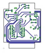
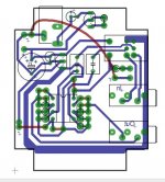
I've attached below a couple screenshots of my board as drawn in Eagle (My first use of Eagle). I did not include part names or values as they are typical of all schematics and because I felt it would make the images to hard to read.
I'll try for a quick explanation of key parts, and if that is not enough I'll try something different. Basically, this will use one 9vdc rechargeable battery and is designed/sized to fit a Hammond 1593PBK (link). It uses a TLE2426CLP rail splitter. Recharge circuit is a LM317LZ and a 47R resistor (NOTE- I may have the pins drawn wrong, I need to check that) and a 1N5819 diode before it to ensure correct powersupply polarity. Zener after the battery in is a 12V/1W 1N4247ATR Vishay to limit input voltage to 12vdc.
Input caps are WIMA MKS2 1uF/63V. The PSU cap is a Panasonic 470uF/25V low ESR e.l. IN and output jacks are vertical Switchcrafts. Pot is a ALPS RK097. The 5 pads next to the pot are for LED and resistor. The red line to ground from each power pin on the IC is for ceramic or similar blocking caps ( could not find a library part that seemed to represent small ceramic caps). Red lines next to IC are jumper wires for potentially needed resistor or caps if IC oscillates. Resistors off of IC from bottom to top (in drawing) are 100K, 2K, 10K respectively. This sets input impedance of amp to 100K and gain of 6.
The other two red lines on the right hand drawing are jumper wires. One for Vcc- and the other for LED negative. I played with many iterations of this and could not do single sided w/o a jumper. I don't think I have the ability to DIY PCB at home using a two sided board. I plan to try the iron-on inkjet toner method.
I'd really like opinion about the traces!! Most are 0.031" (31mil) but the two input from potentometer are 0.024 to fit between the pins. I am anticipating having to trim back the ground pot bads after soldering the pot. Trace clearance everywhere else is at least 0.02". The distance between resistor bads next to IC are ~0.015". Is that enough or should I use smaller pads?
I will say, the screenshots make the pot pads look closer than they do when printed at 1:1 scale. Still, as I said, I am sure I will need to trim the two ground and two output pads back a bit where the clearance is close.
Thanks in advance and thanks to everyone who helped me get this far already.
Thanks to all the terrific help I received in another thread, I have built a couple successful CMOY amps base don the tutorial at Tangents site. Now, I'd like to improve my original builds (or build improved versions) and make a few gifts. I'm using this as an excuse to try my hand at PCB design and etching.
I've attached below a couple screenshots of my board as drawn in Eagle (My first use of Eagle). I did not include part names or values as they are typical of all schematics and because I felt it would make the images to hard to read.
I'll try for a quick explanation of key parts, and if that is not enough I'll try something different. Basically, this will use one 9vdc rechargeable battery and is designed/sized to fit a Hammond 1593PBK (link). It uses a TLE2426CLP rail splitter. Recharge circuit is a LM317LZ and a 47R resistor (NOTE- I may have the pins drawn wrong, I need to check that) and a 1N5819 diode before it to ensure correct powersupply polarity. Zener after the battery in is a 12V/1W 1N4247ATR Vishay to limit input voltage to 12vdc.
Input caps are WIMA MKS2 1uF/63V. The PSU cap is a Panasonic 470uF/25V low ESR e.l. IN and output jacks are vertical Switchcrafts. Pot is a ALPS RK097. The 5 pads next to the pot are for LED and resistor. The red line to ground from each power pin on the IC is for ceramic or similar blocking caps ( could not find a library part that seemed to represent small ceramic caps). Red lines next to IC are jumper wires for potentially needed resistor or caps if IC oscillates. Resistors off of IC from bottom to top (in drawing) are 100K, 2K, 10K respectively. This sets input impedance of amp to 100K and gain of 6.
The other two red lines on the right hand drawing are jumper wires. One for Vcc- and the other for LED negative. I played with many iterations of this and could not do single sided w/o a jumper. I don't think I have the ability to DIY PCB at home using a two sided board. I plan to try the iron-on inkjet toner method.
I'd really like opinion about the traces!! Most are 0.031" (31mil) but the two input from potentometer are 0.024 to fit between the pins. I am anticipating having to trim back the ground pot bads after soldering the pot. Trace clearance everywhere else is at least 0.02". The distance between resistor bads next to IC are ~0.015". Is that enough or should I use smaller pads?
I will say, the screenshots make the pot pads look closer than they do when printed at 1:1 scale. Still, as I said, I am sure I will need to trim the two ground and two output pads back a bit where the clearance is close.
Thanks in advance and thanks to everyone who helped me get this far already.
Attachments
Last edited:
Thanks Digits. It's always nice to see how other people do things.
I guess m two main questions are what is suitable minimum trace width and does my layout look like I would have problems due to interference, etc. Ive tried to lay it out allowing for many potential additions as necessry, such a extra resistors and blocking capacitors in the event of cranky opamps (I'd like to try a bunch of different ones), etc.
Thanks!
If you are etching yoursef with say print and peel sheets, I won't go under .3mm traces. if you have boards made, its no issue and you can probably go down to .1 depending on the fab sepcs, generaly there is not much gained from too thin traces. As you can see, there is provision made for bypassing right at the chip pins for cranky amps (I like playing with the opa2227/8 series).You could make those input caps smaller and put the psu components left of the output jack, and just do two short wire jumpers to V+ and V-. Also those two resistors on the outputs can be low ohm resistors or just wire jumpers if your amps is silent enough.
I've heard really nice things about the 2228 but I ordered a 2227 also. I've tried to find AD825 based on a few reviews but can't find that one. I'll see how the 2227/8 suit me before trying others.
I've tried to leave space on my board design for both extra feedback resistors, output resistors and also parallel caps (for in- resistor) to cover all oscillation fixes I've read about. These can be easily jumpered or used as needed.
Is there a good place to get 2-4 boards cheap in the US? I'd like to make my own but if there is a cost effective solution elsewhere, I'd go that way instead as I don't have any etching abilities at this time and would likely try the toner method with RS etchant or muratic acid/peroxide/salt. I've got enough single sided, 1oz, 1/16" board to make 6 boards (or 6 attempts).
I will almost certainly try the toner method, unless I find some local hobbyist whole do it for me free")
AndrewT, Thanks for chiming in here. The TI datasheet mentions stability issues at gains of 5 or lower. I have found gain 6 to be good for me and my applications using the 2132/2134 opamps, so maybe this will be similar. If not, TI recommends a parallel capacitor to the feedback resistor, which I have allowed space form on my board.
AndrewT, Thanks for chiming in here. The TI datasheet mentions stability issues at gains of 5 or lower. I have found gain 6 to be good for me and my applications using the 2132/2134 opamps, so maybe this will be similar. If not, TI recommends a parallel capacitor to the feedback resistor, which I have allowed space form on my board.
lol, I give my wife the blue press and peel sheets, then email her PDFs of the boards I want, she prints it out and brings it home, I iron it on, wash and peel, and etch, probably takes all of 30 minutes. You get premixed ferric cloride from parts places, put some in an empty glass coffee pot and you can seal and reuse it for ages... just chuck stuff in and swirl around... don't spill, it stains terribly.
Thanks digits. I've read about those sheets but would have to order them and then go someplace with a photocopier or inkjet for printing (taking some reference part or home printed version to double check scale.
What is the minimum trace/pad spacing you would recommend for this method?
What is the minimum trace/pad spacing you would recommend for this method?
Last edited:
Well, thanks for the push. Turns out I have easy access to a laserjet printer. Pulled some pages from the wife's BH&G magazine and gave this a try. I used etchant from Radioshack. Worked really well. I learned I need to prep the copper a little better as I had sticking issues in one spot. I also think I could use a different magazine next time. This one worked but some traces are a little jaggy edged.
I want to make two or three so I am considering this one practice. In hind sight, closer between track tolerances would be fine. My narrowest is probably 0.03" and I'm sure 0.02 would be more than enough space. It's also easy to trim a pad edge back after transfer and before etching with any sharp tool so the occasional really close place could easily be dealt with, as in the area around the alps pot on my schematic.
I want to make two or three so I am considering this one practice. In hind sight, closer between track tolerances would be fine. My narrowest is probably 0.03" and I'm sure 0.02 would be more than enough space. It's also easy to trim a pad edge back after transfer and before etching with any sharp tool so the occasional really close place could easily be dealt with, as in the area around the alps pot on my schematic.
Here is my first board all cleaned up, but not drilled.
I forgot to mention in my last post, Sharpie does work for touch up, but you should do two or three coats and let it dry well between coats. The ground trace issues on the bottom of the image below show where I had that issue.
Any thoughts? Not really looking for kudos here but constructive stuff
Does this look good enough to populate?
Also, I'm trying to figure out if I should tin the traces, spray on some sort of lacquer before or after populating, etc. I read lots of conflicting stuff and not sure what to do. I like the idea that lacquer will help prevent bridging between traces, but not sure if that is true or if I have the right stuff. I've seen some say Krylon clear lacquer or art store fixative (for charcoal drawings) works good before populating, but.... I don't know if that is true. I've read tinning is good and also that it can cause issue with resistance/inductance at the copper/solder interface.
Suggestions?
Attachments
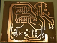
good job for a first go. I see you need to cut open some trace spaces, but otherwise much better than my first attempts. I see you probably have the iron A little too hot... that tends to expand the traces a bit. Somewhere about half of the dial is normally ok, just use more time, of coarse it can also be a side effect of useing glossy pages in stead of the PnP sheets.
But now you can fish, rather than ask for fish, it opens up a new world.
Don't tin with solder, if you want to tin, get a tinning solution. otherwise popluate your boards, clean solder side well with ISO, or a good cycle and dry in the dish washer (wife might not approve of soldering chemicals)... after its dry, and TESTED give the solderside a coat of resin or what have you to stop oxidation.
Re the prepping of boards, important, wash hands to remove oils from skin before starting. Give copper a slight rough texture with a few wipes with medium sandpaper. Then wash and wipe off with ISO to remove any oil traces.
Last edited:
Very well done. Looks pretty good IMO. I agree there's the ground trace issue (no big deal) and the trace separation issue at lower left (easily remedied).
I don't understand a spray coat before populating the board. Never heard of it, and it seems counterproductive. Practice good soldering and inspection techniques to prevent solder bridges. Copper will tarnish of course, and the sprays are convenient "potting" chemicals - when the board is completely finished. There's PCB tinning kits available also if you want to go all out.
Never heard of any copper/solder interface parasitics. Is there not an alloy formed there? I've a lot to learn, but that sounds bogus to me at this point. Maybe it is a real issue.... at 12GHz.
What you may be confused with, is that boards are sometimes fluxed before soldering, it realy helps solder go where it is supposed to, and a real blessing with older tarnished PCBs. Flux must be cleaned off afterwards, as it does cause bridgeing which causes parts of the pcb to become conductive and carbonise (burn), which makes the short more conductive...
Thanks Spud and Digits for the reply.
I'm sure I was not clear. I get what flux does and how/why it is removed afterwards. I have seen mention, in passing, of a spray "lacquer" that also functions as a flux. It keeps oxidation down and is applied before populating. I'm using my phone now to reply so looking it up is annoying, but one product like that was "Something 20" or similar. It seemed Europen in origin and the company had a whole line of products.
I had read an etching tutorial (by Garber at headwize forums) for toner transfer that suggested artist type fixant would do the same thing. This is not the same as the protectant lacquer used after popluating, testing and cleaning.
I don't know if this is true or a good idea but I thought I'd ask. Basically, if the fixative before populating is a good diy trick, I wanted to know. Otherwise, I'm not ordering more stuff. I'll just lightly buff the traces clean, populate, clean, test, etc then add any old nonconducting lacquer afterwards if it is recommended.
Thanks again!.
My parts for these boards will come tomorrow. I'll drill this board and test the pin locations to make sure all is good, then I'll make another board and see if my technique improves.
- Status
- This old topic is closed. If you want to reopen this topic, contact a moderator using the "Report Post" button.
- Home
- Amplifiers
- Chip Amps
- CMOY pcb -my first pcb