Hi,
Newbee in power amp design and construction here, and still much to learn.
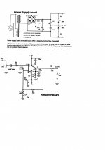
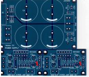
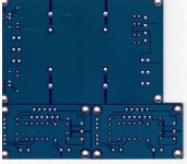
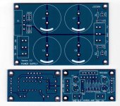
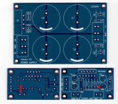
I recently got a PCB kit for two amps and a power supply unit, both unpopulated, that I am planning to solder myself.
As I have absolutely no idea about the different power amp designs and their merits, I thought that I could ask you what you think about these PCBs.
Or, did someone build this same kit?
I am very interested to read you comments.
Again, this may seem as a bottle in the sea, I just do not know where to search.
Regards,
Newbee in power amp design and construction here, and still much to learn.
I recently got a PCB kit for two amps and a power supply unit, both unpopulated, that I am planning to solder myself.
As I have absolutely no idea about the different power amp designs and their merits, I thought that I could ask you what you think about these PCBs.
Or, did someone build this same kit?
I am very interested to read you comments.
Again, this may seem as a bottle in the sea, I just do not know where to search.
Regards,
Attachments
Hi,
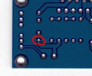
I think you will find that C4 is connected to the signal ground on the top side and to the power ground on the bottom side.
You must break this connection.
Be careful you still have to solder C4 from the bottom side and rely on the bottom pad and the plated through hole to maintain that signal ground connection on the top side.
The bottom pad may be attached to the bottom ground plane by 3 or 4 bridges from the island pad to the plane. You need to very carefully cut these bridges without damaging the pad.
Who told the Chinese that ground planes are equal to or better than star grounding?
Hi,
I think you will find that C4 is connected to the signal ground on the top side and to the power ground on the bottom side.
You must break this connection.
Be careful you still have to solder C4 from the bottom side and rely on the bottom pad and the plated through hole to maintain that signal ground connection on the top side.
The bottom pad may be attached to the bottom ground plane by 3 or 4 bridges from the island pad to the plane. You need to very carefully cut these bridges without damaging the pad.
Who told the Chinese that ground planes are equal to or better than star grounding?
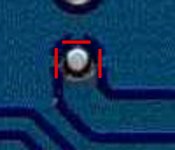
Many thanks for the quick reply.
I am not sure that I understand how to do this.
Which bridges should be cut?
Is the cut (red line) correct?
Regards,
Attachments
Last edited:
normally just some wire wound around it.
I have to apologize for not undestanding the sentence. "Some wire wound around" what?
oops,
there is no output Zobel fitted.
Fit at least the Zobel or preferably the Thiele Network.
__________________
regards Andrew T.
Again, I am just beginning to learn about audio electronics (not even the fist step), I am not sure to understand where and how to "Fit at least the Zobel or preferably the Thiele Network."
May I ask how to do that?
Regards,
I would be interested in any real scientific data on star grounds versus solid grounds, as historicly the star, was a reference to a star point where the analog and digital ground met (today even this practice is not common as one contigous ground is best) as in the intrumentation world of electronics and historicly analoge circuitry has a soldi ground plane. In audio the return current is more problematic as the audio frequencies are where returns are moving from path of least resistance to path of least inductance. Also the skinny looks like an arial (and acts like one) ground schemes that apear also add a lot of parasitic inductance. Add to that the problem of EMC, loop area etc, ground planes are best.
Last edited:
Hi,I am not sure to understand where and how to "Fit at least the Zobel or preferably the Thiele Network."
May I ask how to do that?
The output Zobel is a series pair of resistor + capacitor. Usually it is around 10r +100nF, but National show different values on the datasheet. National also show a number of components as "optional". Beginners must never omit them. All are compulsory.
The Thiele Network is an extension of the output Zobel. Or more correctly the Zobel is a cut down version of the Thiele Network.
An extra parallel pair of resistor & inductor go between the output Zobel and the Speaker Terminals. Some of National's datasheets show this. These two components do not have to be mounted on the PCB. I think they are better mounted away from the PCB, as part of the wiring from PCB to Speaker Terminals.
The Zobel, however, should be mounted on the PCB. as near the output Pin and the PSU zero volts as possible.
Your red line.
No. That is the top side (=side with components mounted when using through hole leads).
Look at the bottom side. find the two pads that link to that same lead. Do they have a trace going to Ground? A better photo of that end of the PCB may show us what is there.
Last edited:
where did you find this historical information?historically the star, was a reference to a star point where the analog and digital ground met (today even this practice is not common as one contiguous ground is best) as in the instrumentation world of electronics and historically analogue circuitry has a solid ground plane.
Balderdash !
Hi,
Your red line.
No. That is the top side (=side with components mounted when using through hole leads).
Look at the bottom side. find the two pads that link to that same lead. Do they have a trace going to Ground? A better photo of that end of the PCB may show us what is there.
I am trying to understand where the C4 is connected to the signal ground on the top side and to the power ground on the bottom side.
As I understand the power ground is connected to the line around the edge of the board (which is by the way very thin on one of the big side).
I see on the back side that C4 is connect to the signal ground. This is what the paper schematic shows. So, I guess that this is correct, or is the schematic wrong?
By the way, by "bottom side", do you mean "back side" or "bottom" as bottom of the picture?
Bit confused here.
Regards,
Attachments
The side with the labels is top side. This is also the side that the components are fitted.
The side with no writing is the bottom side. This is the the side that you do almost all of your soldering.
I can see the trace from C4 to R5 to Signal Ground on the bottom side. I can see the trace from C4 to R6 on the top side.
I cannot see if there are any other connections from these two C4 pads to the bottom ground plane.
I can see the trace from C4 to R5 to Signal Ground on the bottom side. I can see the trace from C4 to R6 on the top side.
I cannot see if there are any other connections from these two C4 pads to the bottom ground plane.
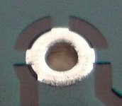
Do you mean like in the picture?
... I still have some difficulty to understand.
Regards,
Attachments
No, not like this.
I can see those two traces connecting C4 to other parts of the input. Those two traces are correct, do not cut them.
Look at the bottom. Find the two pads that solder C4 in place.
One pad has no obvious connection trace. Does this pad connect to the Ground Plane?
The other pad has a trace. Is there another connection to the Ground plane. If there is a little bridge trace from Pad to Ground Plane then that is a connection. I cannot see in the pic. Can you see with a magnifier?
No, not like this.
I can see those two traces connecting C4 to other parts of the input. Those two traces are correct, do not cut them.
Look at the bottom. Find the two pads that solder C4 in place.
One pad has no obvious connection trace. Does this pad connect to the Ground Plane?
The other pad has a trace. Is there another connection to the Ground plane. If there is a little bridge trace from Pad to Ground Plane then that is a connection. I cannot see in the pic. Can you see with a magnifier?
Sincere thanks for helping me, and hope that you will until I get to the end.
I am a bit puzzled by your last question. If we look at the bottom side of the Amp PCB, we see that the pad which is closer to the middle (middle of the PCB) has no connection, as it is connected from the top. The other C4 pad is connected by two traces, indeed.
I use Firefox. Clicking on the thumbnail gives me a zoom on the picture on the whole screen which is by far bigger than using an optical magnifier.
I cannot see any trace connecting the C4 pad on the bottom side.
I still do not understand which bridge is to be cut.
Again, my sincere thanks for your help.
Regards,
Attachments

look at bottom side.
see the Y trace connecting C4 to R5 and to GND.
now look carefully at the C4 lower pad on that Y trace.
There is some blue colour between the hole and the Ground Plane (I cannot see clearly). Are these blue marks on the pic, copper bridges between the Pad Island and the Ground Plane?
Get your magnifier out and "LOOK" at the bottom of the PCB.
Go back and read post 2. It describes what to look for and to be careful if you "find" these bridges.
Last edited:
")
look at bottom side.
see the Y trace connecting C4 to R5 and to GND.
now look carefully at the C4 lower pad on that Y trace.
There is some blue colour between the hole and the Ground Plane (I cannot see clearly). Are these blue marks on the pic, copper bridges between the Pad Island and the Ground Plane?
Get your magnifier out and "LOOK" at the bottom of the PCB.
Go back and read post 2. It describes what to look for and to be careful if you "find" these bridges.
My confusion may find its source in the words used and my ignorance in PCB conventions:
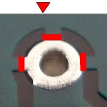
- the C4 lower pad is surrounded by a blue trace that form a cross. Does this cross mean anything special?
- by GROUND PLANE, do you mean that the power ground extends over the entire PCB surface, BELOW the traces connecting the components?
Regards,
Attachments

yes, that is something special.
The unpainted part is the solder pad.
The "Cross" is a copper connection 3 of them) to the surrounding copper plane (Ground Plane).
The spaces between the cross bridges are there to allow easier soldering of the pad.
The pad has a trace from the bottom. The pad and trace must remain undamaged.
The surrounding Ground Plane is of little (more accurately of absolutely no purpose) importance in this area.
Cut the 3 bridges that span from island to surround.
First cut right out at the outside of each bridge next to where it meets the surrounding copper.
I use a very sharp craft knife and press down heavily slightly off vertical, the blade point into towards the bridge.
The second cut for each bridge should be at about half way across the bridge, but this time the blade is angled slightly towards the surrounding copper. If you are very lucky you may find that the two angled cuts "lift" a tiny sliver of copper clean off the substrate. You may have to force the sliver off by using a very angled blade and push hard safely to get it to lift clean off. be careful, a very sharp knife and some hard pushing can make a big hole in your hand/finger.
The island pad with one trace off to the bottom should now be electrically isolated from the Ground Plane. Check it with a resistance meter. Get the magnifying glass out and check there are no loose pieces of copper trace that could short out later.
Now check that the bottom trace is electrically connected to the top pad. This is important or the amplifier will not work.
You have now separated the Signal Ground from the Power Ground.
Later you need to reconnect these with a wire and/or resistor at a better location.
yes, that is something special.
The unpainted part is the solder pad.
...
Cut the 3 bridges that span from island to surround.
First cut right out at the outside of each bridge next to where it meets the surrounding copper.
I use a very sharp craft knife and press down heavily slightly off vertical, the blade point into towards the bridge.
The second cut for each bridge should be at about half way across the bridge, but this time the blade is angled slightly towards the surrounding copper.
Ok. The bridges have to be cut in a V-shape as is shown in the picture, is it correct? The red triangle at the top of the picture represents the cut profile.
As I do not possess any craft knife nor any surgical scalpel, I will try with a razor blade. I hope that I am sufficiently skilled to not loose a finger in the operation.
I do have a multi-meter, so it will not be a problem to check the electrical connection.
You have now separated the Signal Ground from the Power Ground.
Later you need to reconnect these with a wire and/or resistor at a better location.
? That I do not understand. I am tempted to ask why reconnect when the primary goal of the operation was precisely to disconnect them. I assume that it has to do in some way with the Thiel network.
Regards,
Attachments
- Status
- This old topic is closed. If you want to reopen this topic, contact a moderator using the "Report Post" button.
- Home
- Amplifiers
- Chip Amps
- Low cost Power Amp PCB from the net (LM3886) - what do you think of the schematic?