Here are the exported images of the schematic and layout - hope it uploads from my GPRS phone.
It looks like the ground-planed areas got left out, on the PCB layout.
Hey linuxguru, do you have a recommended BOM?
You can safely go with the same parts as the corresponding ones on the Myref Rev C monoblock BoMs. The few parts that differ are the relay, chipamp, opamp and the compensation cap (styroflex or C0G ceramic).
It looks like the ground-planed areas got left out, on the PCB layout.
It shows only the outline of the ground plane on the exported image. However, if you run the CAM processor on the uploaded Eagle .brd file (e.g. to generate a set of Gerbers), the ground planes will be correctly rendered on the Gerbers. This can be verified using a Gerber viewer like gerbv.
Interconnection circuit containing transistors Q1, Q2 and Q3 with the rest of the circuit is defective, or otherwise, is not right. Something is wrong here, namely: on each LM1875 output potential is zero (in theory, neglecting offset), then you should not connect the electrical potential across the audio overlaps directly with certain points, dc voltages from the circuit with Q1 ... Q3.Here are the exported images of the schematic and layout - hope it uploads from my GPRS phone.
That would be the biggest mistake.
And another mistake - should be tested to see if it's so - is that the output voltage alternative to LM's, its RMS value, if it exceeds a certain value could go in conduction transistors Q1 .. Q3.
And another mistake - should be tested to see if it's so - is that the output voltage alternative to LM's, its RMS value, if it exceeds a certain value could go in conduction transistors Q1 .. Q3.
Q1, Q2 and Q3 are part of the speaker DC-protection circuitry only - their main function is to open the relay when the output DC offset crosses a certain threshold. It's a proven circuit, similar to that used in the MyRef Rev A-C, so it most probably will work perfectly as shown or with a few minor tweaks to the values of resistors.
To understand the amplifier topology, just ignore the protection circuitry.
DC circuit protection with those transistors Q1 .. Q3 I don't think it will work properly.
It works fine in the MyRef - there isn't a single reported case of blown speakers due to a failed DC protection circuit in the MyRef.
In any event, the schematic and layout are free to modify - you're welcome to use a uPC1237 or anything else to implement a better DC protection circuit if you wish.
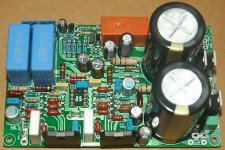
Here's a pic of the first MiniRef 3886 prototype, almost completed. It has since been completely assembled and powered up safely today. It's stable and working as designed, thus validating the nested Jung-Howland-Penasa chipamp topology.
The image is missing! Must see...
does the output offset at each 3886 outpin vary when the opamps are swapped?
Do the two 3886 offsets always match and to what discrepancy/tolerance?
I can't easily swap left and right opamps since it's a dual DIP8 - the only way to do it is with 2 SOIC8 opamps on a Brown Dog or similar. However, for any specific opamp type (say OPA2134) the variation seems to be no more than +/- 50 per cent or so.
The variation between channels can be large - with the JRC4560, one channel shows about 4 mV, and the other about 0.8 mV. However, this could be due to external resistors, etc.
Other than the static output offsets posted earlier, no measurements yet. The good news is that it is stable or could be made stable with a fairly wide representative sample of dual DIP8 opamps, with very minor tweaks. I have a very similar 2nd prototype in the assembly stage with LM3876, instead of LM3886, for comparitive testing. I hope to audition both shortly.
- Home
- Amplifiers
- Chip Amps
- MiniRef Schematic and PCB layout