Hi all!
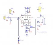
I've decided to go a little bit different on this one, because I've heard one LM3886 that is built on this topology and it sounds awesome. So can you tell me if this will work or if I can ran into some problems. There is also current source on the output, made with LM317, now rated at about 430mA, but it will be lowered to 100mA.
Regards Aleš
Attachments
I don't see the point of the LM317 current source other than making a huge dc offset on the output.
Why would it make huge DC offset? Anyway can I omit feedback capacitor if I am going to use input cap?
Regards Aleš
Why would it make huge DC offset? Anyway can I omit feedback capacitor if I am going to use input cap?
Regards Aleš
The LM317 circuit is apparently to drive the output stage into class A at low levels. The LM3886 sounds quite clean at low levels and so you might skip that part or make it on a smaller ( daughter) pcb and removeable if you find it doesn't really make a diff.
Wonder what the idea was as the current will only affect one output transistor.
I remember trying the amp without the feedback cap. DC offset went up to about 0.1V or thereabout. But it worked fine ....better sound without the cap. I did use a good film cap at the input.
Your feedback resistor ( 1 K ) is much lower than the input resistor ( 22K). Assuming equal bias currents in the input stage you might get a greater differential in the voltage drop between these two resistors and cause a higher offset at the output. Do check it with 1K and 22K . ( 47 ohms will also have to change to about 1 K to keep the same gain ).
Last edited:
The LM317 circuit is apparently to drive the output stage into class A at low levels. The LM3886 sounds quite clean at low levels and so you might skip that part or make it on a smaller ( daughter) pcb and removeable if you find it doesn't really make a diff.
Wonder what the idea was as the current will only affect one output transistor.
I remember trying the amp without the feedback cap. DC offset went up to about 0.1V or thereabout. But it worked fine ....better sound without the cap. I did use a good film cap at the input.
Your feedback resistor ( 1 K ) is much lower than the input resistor ( 22K). Assuming equal bias currents in the input stage you might get a greater differential in the voltage drop between these two resistors and cause a higher offset at the output. Do check it with 1K and 22K . ( 47 ohms will also have to change to about 1 K to keep the same gain ).
I've used LM317 on the output so that the circuit stays simple and you can use it with different voltages without changing anything, if I will have any problems with LM317 then I will try with transistor, BD139 maybe. The feedback resistor is low because, as said before, I've heard one with this kind of values and it was really neutral and of the best I've heard. For the start here is the first PCB drawing I made today with input cap. If anyone has any idea on PCB improvment, hit me
 , before I make one in couple of days.
@AndrewT: Maybe I should put resistor between signal GND and GND, but I will see if the amp will be dead quiet, then I will leave it this way.
Regards Aleš
Attachments
Maybe you should read Doug Self's work on distortion in amplifiers where he shows that a richly biased Class AB output stage like you are making here actually has higher distortion than a plain old Class B output stage due to gm doubling effects.
By biasing the chip like this you intuitively think that you're getting a bit of Class A performance, but you're not really.
By biasing the chip like this you intuitively think that you're getting a bit of Class A performance, but you're not really.
I'm not convinced that resistive loading the output gives rise to gm doubling. That occurs when the bias current is fed down through both transistors in the output stage. Here, only one transistor sees the extra current, not both. The output stage of an LM3886 is quasi-comp anyway, can gm doubling apply to such stages?
Your point about higher distortion may well stand nevertheless, its unwise to increase the loading of a chip amp, they're already pretty heavily challenged in the thermal dept.
Your point about higher distortion may well stand nevertheless, its unwise to increase the loading of a chip amp, they're already pretty heavily challenged in the thermal dept.
New PCB is on the way, with star grounding very close to the pin7. The CCS on the output will be added extra, if won't do any good then CCS no go. The feedback resistor values are also changed, because the 1kE/47E are problematic even with DC(I am getting about 30mV on the output), but with 10kE/470E works ok(the only pair I have at home). On the psu lines there will be only 1uF or 470nF capacitor per line(because it's very hard to make star gnd pcb).
Regards Aleš
Regards Aleš
I think published PCB will now be the final. I still have to make a prototype to see how it sounds. I didn't use bypass caps because they have no funtion here. If the cap C4/C6 have resistance less than 0.5 then the impedance of 100nF gets lower above 3MHz frequency, amplifier doesn't do much in this range. Feeback resistor R7 will be soldered directly on the pins to decrease inductance loop. The C1 cap is now connected to the ground, because if soldered to pins 9 and 10 it gives amplifier great stability, but it decreases the following speed of input signal. I will use input cap but it will be mounted off board. PSU will be dual mono, so that the star ground on the PCB has it's effect.
Regards Aleš
Regards Aleš
Attachments
So I made PCB that is published in previous post and I have tested it, at first I had some problems with ground noise which was produced by R6, so this resistor is now removed. The PSU is dual mono made out of SMPS Meanwel, 12V(18W) per line and it plays really good. The bass is really low and controled, the highs are nice and not pushy, really detailed, also the mids are really good. I will post some pictures when the project will be finished.
Regards Aleš
Regards Aleš
Attachments
- Status
- This old topic is closed. If you want to reopen this topic, contact a moderator using the "Report Post" button.
- Home
- Amplifiers
- Chip Amps
- New LM3886