I visit DIY Chip Amplifier Kits, PCB's, Components and Information. and found lm3886 pcb it is
a) Red color ( Is that paint or what is ? )
b) Solder at component side ( How is it possible ? )
c) DIY Chip Amplifier Kits, PCB's, Components and Information. is also make pcb by this toner procedure ?
red color is the protective coating, normally it is green color for PCBs
solder at component side - its a double layer PCB, so u have copper in both layers.
and chipamp is a professional PCB provider, he use more sophisticated machines for PCB making
")
( i guess u are quite new in this field )
-By the way i feel 5 mins of heat is too high. My setting is 1.5 mins with normal amount of pressure. Keep 10 layers of newspaper below pcb, then place the pcb with copper side facing on top, put the glossy paper and again keep 6-8 layers of newspaper. and try to keep PCB small enough so that it can be contained with in the cloth iron. just apply for 1.5 mins at full heat and moderate hand pressure.
I might have missed it, but did you thoroughly clean the copper of the PCB? I thoroughly scrubbed the copper side with a synthetic scrubbing pad and then cleaned with 99% rubbing alcohol or acetone with white paper towels until the paper towels stopped picking up dirt. This took several minutes.
I then printed from expresspcb on some glossy ink jet paper in my laser printer. I'm using a brother laser with a brother toner cartridge.
If you get no toner transfer, you are printing on "ink jet" paper using a "laser printer", correct? That's the only way this method works.
I actually tape the PCB to the the glossy paper before ironing to ensure the paper doesn't move with respect to the PCB.
I had the iron on "high" or "cotton" setting and made sure I the whole board got evenly heated and made sure to use the nose of the iron to press on the traces to help. This should only take a few minutes.
It worked like a charm for me. In fact the paper lifted away immediately without soaking. I ended up couple minor pinholes and there was some paper material between closely spaced traces that I used a blade to remove.
I agree, it may be best method and I need little practice to get right time, heat and pressure to use with iron.
Okey. Today I tried, but all circuit does not appear on pcb. I think there is no confusion till circuit printed on glossy paper. Please find what is my mistake.
1) I put pcb copper side up on the piece of MDF.
2) printed glossy paper, printed side at copper.
3) Put the iron on the paper upto 5 min. ( There is no way to find circuit appear on pcb or not. Because paper stick with pcb. If circuit not appear on pcb more heat required )
4) After 5 min. I found glossy paper is still white, (means, heat does not effect) PCB becomes very hot & little BEND. after 2 min I put it in full glass of water. After 10 Min glossy paper removed very easily but few part of circuit does not appear on pcb.
I think, equal pressure & heat is required to all the area of pcb. OR what ?
It sounds like pra3718 either didn't get the board cleaned well-enough or didn't use enough pressure with the tip of the iron. It also is necessary to roughen the copper surface a little bit, before you clean it, with a very fine-grain abrasive, such as a fine-grain synthetic scrubbing pad.
And it's not "equal pressure...to all parts of the pcb" that you want, pra3718. Keeping the iron flat is usually not enough pressure. So (after heating the whole thing with the iron flat) you should probably try using just the part near the tip of the iron, and move it across only part of the board at a time. You would basically be moving it along "rows and columns", i.e. vertical strips of the board and then horizontal ones, reheating the whole board periodically if necessary (maybe necessary for large boards; it's "trial and error" until you get a feel for it.).
At least you can always wash the toner off with Laquer Thinner and start over.
Cheers,
Tom Gootee
Yes, this time done it.
1) Artwork printing should be FULL-IN-DARK-MODE.
2) Copper side board should be cleaned.
3) "Keeping the iron flat is usually not enough pressure. So (after heating the whole thing with the iron flat) you should probably try using just the part near the tip of the iron, and move it across only part of the board at a time" that's true.
This way I can make PCB at home. But sorry, not professional looking. it looks like home-made pcb. I never tried screen printing but toner transfer & screen printing method should be in same result. or what ?
I wish to know how to make professional looking pcb?
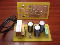
Hey, why don't u try my LM3886 diy PCB, http://www.diyaudio.com/forums/chip...ngle-sided-diy-pcb-lm3886-power-supply-2.html is the link.
just print the pdf and transfer it on copper board
And i asssure you , with toner transfer method , u can make high quality PCBs.
just print the pdf and transfer it on copper board
And i asssure you , with toner transfer method , u can make high quality PCBs.
And i asssure you , with toner transfer method , u can make high quality PCBs.
Yep, you can count on it. The final result will look very good.
A way to make it even easier is to Google "Press n Peel Blue" from techniks dot com.
Using a laser jet you print on the rough side. Using a stanard iron at just below steam transfer it over to the clean pcb.
The attached photo is a recent board I made for another project using Eagle light and the press n peel. The traces in this case are pretty thick, but I have made then as small as 0.05 before without too much problem. It works ALOT better than simple toner transfer.
Attachments
Hello friends and gurus,Iam new here. Can any one say where i can get pcb clads for my projects. Iam staying in south India, Andhra pradesh. Please sirs Iam in need of it mostly. If any one of u sent me in corrier I can pay. Please help.
patnaik_kottakki,
Hopefully, someone from your area will post here with more-suitable information for you. But you could try on line:
ebay.com - search for "FR4". (Maybe try google.com: "India FR4".)
You could also look at mouser.com, and many other similar electronic component distributors.
Cheers,
Tom
If you are good at freehand drawing you can easily trace the PCB layout on the copper clad laminate using a OHP aka permanent marker. A Fabre castell or Luxor one will do. I have etched even elaborate PCBs using this method. A ruler and a stencil will be helpful for shaky hands. After completing the drawing just immerse in etching solution.
No toner transfer or photoresist methods required especially in the small pcbs used for chip amps. One case also try using adhesive tape, ruler and a paper cutter.
No toner transfer or photoresist methods required especially in the small pcbs used for chip amps. One case also try using adhesive tape, ruler and a paper cutter.
To do what AVbuilder suggests , it will be a good idea to print the design on a paper ( copper side) and place it on the bare pcb and drill all the holes. Then remove the paper and paint up all the tracks and pads. If you have a reasonably steady hand this isn't hard to do.
If you can't get your OHP marker you can also use nail polish and use a nail polish thinner ( or amyl acetate) to thin the nail polish. Use a fine tipped brush to apply. Can't get one fine enough ? Just get the thinnest and trim it to size ! A good OHP marker is easiest but better check if the type you get is really resistant to the etching process. A small test pcb would tell you. With the OHP ink you might need to go over the tracks two or three times to ensure that enough ink has been applied.
NC paint thinner will also dissolve the nail polish but amyl acetate evaporates more slowly and so you get more time to apply before the nail polish starts to get too thick again.
Last edited:
amyl acetate was easy to google. Melting to boiling range ~ 220C degrees, that's quite big. The 149 boiling point explains why it evaporates more slowly.
NC paint thinner not so obvious. Almost all search results came from India, I wonder why.
Turns out NC probably = nitro cellulose
NC paint thinner not so obvious. Almost all search results came from India, I wonder why.
Turns out NC probably = nitro cellulose
- Status
- This old topic is closed. If you want to reopen this topic, contact a moderator using the "Report Post" button.
- Home
- Amplifiers
- Chip Amps
- etching gainclone pcb