")
I have only glanced through the layout.
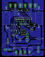
I would have added 0,1uF decoupling caps right across the supply pins of LME49830 to Pwr Gnd. Look at this: http://www.diyaudio.com/forums/showthread.php?s=&threadid=132179&perpage=25&pagenumber=6, Post 126.
I would also move the connection of the NFB resistor right to the speaker terminal.
No VBE multiplier? No pot to set bias???!! Hmmm, I wouldn't even have tried that.
Good luck!
Oh yeah the feedback resistor would work better near the output.
And about the caps to ground im a bit confused on that one. He is talking about power and signal ground. The power ground is far away from the chip so i think that would render the to ground caps a bit noneffective to the LME. But dosent the main supply for the LME come from between the positive and negative supply where i have put a big film cap right next to it.
About the bias i plan to first solder a pot on wires to set the bias and replace with a fixed resistor when i know the value.
As for what i read from the documentation BJTs need a temperature compensated bias since they like to do thermal runaway while MOSFETs don't.
As for what i read from the documentation BJTs need a temperature compensated bias since they like to do thermal runaway while MOSFETs don't.
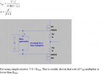
This is true for lateral MOSFET's but not for IRFP's which are of the vertical type. My advice is to use VBE multiplier as decribed by the AN.
dosent the main supply for the LME come from between the positive and negative supply
True, but decoupling both neg. and pos. supplies to power ground is imperative to achieve stability. The single cap you have is not likely to be enough, and it's to far away from the chip terminals. Put a ground connection path driectly from the GND connection and place the decopuling caps as close as possible to the chip terminals.
Pin 10 is not connected to -V trace coming from the bottom.
It seems you don't leave any room for LME heat sink. As Segran suggested, you should have, say, 0.1 uF decoupling cap right next to Pin 15, 10. You connect pin 2 directly to the zener diode? You should add a resistor to set the current. You should put a small cap at input to filter RF signal. It seems that you parallel NFB E-cap Ci and Ri. They should be in series! Please check your schematic against circuits shown in data sheet / app note.
You put a cap across +V and -V. Why?
The more i look at the app note the less it makes sense to me, now i noticed the PCB in the app note has no connection between power ground and signal ground and has those caps on signal ground that caused that members amp to become unstable.
Also i don't get why you would use a thermal bias compensation transistor on a MOSFET since according to the datasheet of the IRFP240 as the temperature rises its resistance rises also so reducing the bias current if we use bias compensation it would additionally reduce the bias even more. So i don't really see the point. I know BJTs will start hogging even more current as they get hot so its logical to lower the bias to counter it.
Also i don't get why you would use a thermal bias compensation transistor on a MOSFET since according to the datasheet of the IRFP240 as the temperature rises its resistance rises also so reducing the bias current if we use bias compensation it would additionally reduce the bias even more. So i don't really see the point. I know BJTs will start hogging even more current as they get hot so its logical to lower the bias to counter it.
berni8k said:
Also i don't get why you would use a thermal bias compensation transistor on a MOSFET since according to the datasheet of the IRFP240 as the temperature rises its resistance rises also so reducing the bias current if we use bias compensation it would additionally reduce the bias even more. So i don't really see the point. I know BJTs will start hogging even more current as they get hot so its logical to lower the bias to counter it.
I think you are referring to the on resistance of D-S. You should look at Vgs vs temperature which is bias related (Vbe vs temp for BJT). Temperature tracking not only for avoiding thermal runaway, but also for stable bias point. Please read AN-1645.
Well actually no because i decided to go D-Class.
I have decided to use the TAS5630 from Texas Instruments, its a 600W D-class amp ic inside a tiny SSOP44 chip and runs off a single 20-50V supply.(I have done lots of tiny SMD soldering and board etching so its no problem.)
What convinced me in to that is its simplicity. All the chip needs is a few caps and resistors around it along with a small inductor on each output. It has everything in it, form a input buffer( takes differential too) to the modulator and the power output stage. In BTL mode it outputs two 300W channels and THD stays under 0,05% over half the way there.
Oh and i don't plan on actually using the 600W per chip (Would be a "little" too loud) But i like having the extra headroom also at low powers (For this amp 50W per channel is still low power) the chips should stay piratically cold.
If you people are interested in a homemade 600W D-class i can post up the PCB drawing and updates about it.
Well this chip was just recently released (TQFP packege is not avalable yet)
In the description of the device Texsas talks about PurePath™ HD technology and the feedback it provides.
So yeah from this it almost looks like why bother with the hot AB amps.This is the performance of a AB with near no heating of a D-class along with the simplicity of a chip amp. Only thing is that you need SMD experience to etch a board and solder it. I solder these 0,65mm SMDs without any specialized SMD tools (soldering iron with pointy tip,flux and some solder wick)
In the description of the device Texsas talks about PurePath™ HD technology and the feedback it provides.
PurePath™ HD technology enables traditional AB-Amplifier performance (<0.03% THD) levels while providing the power efficiency of traditional class D amplifiers.
PurePath™ HD Enabled Integrated Feedback Provides:
* Signal Bandwidth up to 80kHz for High Frequency Content From HD Sources
* Ultralow 0.03% THD at 1W into 4
* Flat THD at all Frequencies for Natural Sound
* 80dB PSRR (BTL, No Input Signal)
* >100dB (A weighted) SNR
* Click and Pop Free Startup
So yeah from this it almost looks like why bother with the hot AB amps.This is the performance of a AB with near no heating of a D-class along with the simplicity of a chip amp. Only thing is that you need SMD experience to etch a board and solder it. I solder these 0,65mm SMDs without any specialized SMD tools (soldering iron with pointy tip,flux and some solder wick)
Hi,
mosfets of the type you have quoted, irfp240, always need bias temperature compensation.
These are Vfets.
They behave in a similar way to BJTs in this respect.
Only the Lfets can be used with a resistor type bias voltage generator.
Lfets are usually expensive and most builders avoid simply because of the cost.
pm pdf please
Hmm... i did attach it why didnt it upload.
Lets give it a another try then
Oh yeah the feedback resistor would work better near the output.
.
|The feedback resistor path should be as short as possible.
This is a critical component path.
1mm = 1nH of inductance and can lead to oscillation.
- Status
- This old topic is closed. If you want to reopen this topic, contact a moderator using the "Report Post" button.
- Home
- Amplifiers
- Chip Amps
- LME49830 PCB design