Hi all,
Just finished laying out this board. Its based on National Semiconductors bridge/parrallel amplifier schematic (figure 13) from the document http://www.national.com/an/AN/AN-1192.pdf.
Id very much like some feed back and people to check I havent made any mistakes before I send it to be made.
Parts match that on page 18 of the AN-1192 document
Configurations options of the board:
BPA 200 with servos
BPA 200 without servos
4 single LM3886 (stereo bi-wire) 4 seperate ins and outs
Attached should be a PDF of the top + bottom + silk
Thanks for looking
Attachments
Looks, as if you had skipped a bunch of capacitors. There only seems to be one of the eight 100 nF decoupling caps (Cby2) on the board. The missing ones can still be soldered directly to the IC pins, but where do the 470 µF (Cby5) go? The two 3300 µF capacitors on board are not replacing the eight 10000 µF capacitors recommended off board in the application note, are they?
Four separate muting circuits can lead to strange behaviour at the speaker terminals. The capacitor tolerances will lead to unsynchronized activation of the four amplifier channels. One Rm/Cm combination that acts on all channels would be better.
There seem to be three missing connections. RF4 to its corresponding output, RD1 to CD1 and Rb3 to CB2.
isolation for the ground polygon is too small, you need to increase the isolation(clearance between components not connected to ground and ground plane ). PCB maker might not be able to work with this much tolerance.
IMHO ground plane type design is not preferred especially for high power amp designs...national mentions the same on their application note on LM4702 based power amp design.
IMHO ground plane type design is not preferred especially for high power amp designs...national mentions the same on their application note on LM4702 based power amp design.
Thanks for the feedback pacificblue and sasmit! Much appreciated.
I have so far corrected:
The 7 missing CBY2
Removed 3 of the muting circuits and join U1,U2,U3,U4 to a single muting circuit I guess the values will now be quiet different? Each chip needs to draw 0.5 mA so all 4 together will 2mA right?
Sorted the three missing connections.
Having done that this just leaves the 470uf caps and ground plane.
These two issues require a major redesign i.e. a bigger board to accommodate 8 470uf (12mm in diameter the smallest I could find for 50V) in there various places close the IC would be best I guess?
The 3300uf were just there as extra to make up for the 2 73800uf supplies in my 2 BA100 amps. I was going to use one per channel for the BPA200 this should be enough. Do I need the extra 3300uF? I guess 8 470uF close to the pins would be better than 2 3300uF?
Thanks again guys for the help.
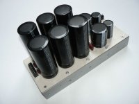
Attached a pic of the current supplies for those interested")
I have so far corrected:
The 7 missing CBY2
Removed 3 of the muting circuits and join U1,U2,U3,U4 to a single muting circuit I guess the values will now be quiet different? Each chip needs to draw 0.5 mA so all 4 together will 2mA right?
Sorted the three missing connections.
Having done that this just leaves the 470uf caps and ground plane.
These two issues require a major redesign i.e. a bigger board to accommodate 8 470uf (12mm in diameter the smallest I could find for 50V) in there various places close the IC would be best I guess?
The 3300uf were just there as extra to make up for the 2 73800uf supplies in my 2 BA100 amps. I was going to use one per channel for the BPA200 this should be enough. Do I need the extra 3300uF? I guess 8 470uF close to the pins would be better than 2 3300uF?
Thanks again guys for the help.
Attached a pic of the current supplies for those interested
Attachments
Right.bm0rg said:Each chip needs to draw 0.5 mA so all 4 together will 2mA right?
Absolutely.bm0rg said:I guess 8 470uF close to the pins would be better than 2 3300uF?
PCB V2
Hi,
Ok here is V2 with the corrections. The layout is a little different and some how ended up being a little smaller.
CBY5 and CBY2 are all as close to the pins as I could get them.
For the muting circuit if I have a power supply of +/- 36 v dc which if I calculated correctly Rm should equal 16700 ohms so I guess a 16k or 15k resistor?
Cm I believe softens to mute on/off. 100uF ok?
Thanks every one for the help so far.
Attachments
Hi,
try dropping the mute resistor to 10k.
That will pass 3.6mA @ 36V. That is 0.9mA/device.
The absolute min mute current is 0.5mA, but I don't know what tolerance National has achieved on this value. If 10k does not pass sufficient current one or two of the devices might not turn completely on.
Cm creates a delay in the mute. This gives time for the circuit to settle before output is passed.
The 100nF must be very close or even on the supply pins. You are almost there, hopefully the ground plane under the device pins will let these fast pulses find the shortest route. It might help to remove the NC pins and clear the ground plane at these three locations.
The x00uF can be a little further away from the supply pins, you are OK here.
RD2 is not connected to CD1. Rf2 is not connected to its corresponding output. Does your layout software not allow for a Design Rule Check?
The CBY5s for the negative rail seem to be touching the heatsink. Capacitors don't like heat. Allow for a little space between capacitor and heatsink.
The CBY5s for the positive rail might be in the way, when you try to tighten the screws through the LM3886s.
The fixing holes seem to be very close to components or pins. Remember that screw heads need space and that they must not produce shorts.
bm0rg said:Thanks AndrewT pacificblue for your help and advice, much appreciated.
ok i think this is it.
Here is the top + bottom and silk
Dear bm0rg,
Sorry to discourage you, but don't use ground planes in this design. I've done it bin there... I designed a bridge/parallel amplifier with 6 LME3886's with a ground plane. As result I had a slight hum and induced noise. THD+N increased. Currents will flow over the ground plane and can get (together with noise) into the chip via it's ground pin, or shorted negative input which refer to the same "dirty" ground. You need a proper star grounding, and the ground pin from the chips should lead separate to the star ground.
My second design was with star grounding and noise and hum where gone, and THD+N went from 0,03% to 0,007%
Ground planes are more for digital and low level circuits. Not for high power current demanding amplifiers.
With kind regards,
Bas
thanks pacificblue & Sebastiaan for your replies.
Yes the output track is close to the input track a little alteration here should be easy to do thanks for the spot.
So from what I gather I need a power ground for this "dirty ground" and a separate ground for the ground pins of the 4 lm3886O
I guess the dirty ground can be still connected to the power supply 0 volt rail but where would the ground for the lm3886 go if they should be grounded separately?
Sebastiaan said:
Dear bm0rg,
Sorry to discourage you, but don't use ground planes in this design. I've done it bin there...
With kind regards,
Bas
I also have experienced similar issues ...even National mention the same....I recommended the same changes when I saw the design ...
if you have a look at national's reference pcb for 4780 you'll find they have isolated dirty and clean ground and star grounded in a nice way but lot of people here say national's pcb is not at all good..I designed a pcb on simmilar lines and I can barely hear the amp when it's on..no hiss no hum at all.
In fact the first time I switched it on for testing i thought it's dead..and turned the pot all the way up ..just to get blasted when I fed a signal.
In fact the first time I switched it on for testing i thought it's dead..and turned the pot all the way up ..just to get blasted when I fed a signal.
Have you also noticed that the same people often are searching advice, because their own PCB designs don't work?sasmit said:lot of people here say national's pcb is not at all good.
- Status
- This old topic is closed. If you want to reopen this topic, contact a moderator using the "Report Post" button.
- Home
- Amplifiers
- Chip Amps
- BPA200 / Stereo Bi-wire PCB V1