
boosting the output current
thanks for the info about the lme49811, etc....I'll have to play around with those.
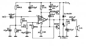
If you're looking for more current drive, you could do something like this. Please note...it's a concept drawing...some components are omitted...the basic idea is that at low output currents, most output comes from the national part, as output current demand increases, the output transistors kick in above about 0.4 Amps. You'll need to experiment some for stability considerations...just consider this as a suggested starting point...
thanks for the info about the lme49811, etc....I'll have to play around with those.
If you're looking for more current drive, you could do something like this. Please note...it's a concept drawing...some components are omitted...the basic idea is that at low output currents, most output comes from the national part, as output current demand increases, the output transistors kick in above about 0.4 Amps. You'll need to experiment some for stability considerations...just consider this as a suggested starting point...
Attachments
It would be very impractical to use analog for high powers. The thermal dissipation would become a big problem (watercooling needed) and the power supply would be very expensive. A pure or hybrid digital would be a better solution.
TI has a pure digital chipset (TAS5261 power stage + TAS55xx digital driver) good for over 200W. Use a discrete power stage and it can be even higher. Only small heatsinks would be needed
TI has a pure digital chipset (TAS5261 power stage + TAS55xx digital driver) good for over 200W. Use a discrete power stage and it can be even higher. Only small heatsinks would be needed
I know I'm bit too late for this party from 2009. Anyway better late than never !
As an experiment I first tried to couple output transistors NJW0281 NJW0302 through 5W resistors to TDA7293
1) in the output stage
2) in the +ve & -ve rails
Used toroidal Transformer 25 0 25 600VA. Output DC at +38 0 -38 with 10A fuse on both rails
The circuit works fine only with TDA7293 i.e.: if the output transistors are not connected. As soon as the transistors are connected the circuit goes into oscillation with loud hum blowing the fuses. If the one fuse fails first the TDA7293 just explodes !
After blowing up 5x TDA7293s I decided its not my cup of tea.
Then I tried with LM3886 with output transistors in the +ve & -ve rails but the circuit was still oscillating sometimes when connected blowing the fuses. The good thing was nothing explodes because of the internal protection of LM3886 - which was a relief ! Then it dawned on me to replace the output transistors NJW0281 & NJW0302 with 2SC5200 & 2SA1943. Voila ! the circuit works however the issue was thermal dissipation due to higher quiescent current of LM3886.
Shifted the circuit to LM3876 which has lower quiescent current. Used LM3886 XY ebay amp board with output transistors in the +ve & -ve rails. At high bass levels the LM3876 dissipates much more heat w.r.t to output transistors.
But again for Subwoofer duty by altering the power resistors one can reduce the thermal dissipation at the cost of bandwidth /slew rate. Managed to even out heat by increasing the power rail resistors & adding a output resistor for LM3876
LM3876 / LM3886 with 2SC5200 & 2SA1943

Left LM3876 on XY pcb - Right LM3886 on Wintek pcb (local)

As an experiment I first tried to couple output transistors NJW0281 NJW0302 through 5W resistors to TDA7293
1) in the output stage
2) in the +ve & -ve rails
Used toroidal Transformer 25 0 25 600VA. Output DC at +38 0 -38 with 10A fuse on both rails
The circuit works fine only with TDA7293 i.e.: if the output transistors are not connected. As soon as the transistors are connected the circuit goes into oscillation with loud hum blowing the fuses. If the one fuse fails first the TDA7293 just explodes !
After blowing up 5x TDA7293s I decided its not my cup of tea.
Then I tried with LM3886 with output transistors in the +ve & -ve rails but the circuit was still oscillating sometimes when connected blowing the fuses. The good thing was nothing explodes because of the internal protection of LM3886 - which was a relief ! Then it dawned on me to replace the output transistors NJW0281 & NJW0302 with 2SC5200 & 2SA1943. Voila ! the circuit works however the issue was thermal dissipation due to higher quiescent current of LM3886.
Shifted the circuit to LM3876 which has lower quiescent current. Used LM3886 XY ebay amp board with output transistors in the +ve & -ve rails. At high bass levels the LM3876 dissipates much more heat w.r.t to output transistors.
But again for Subwoofer duty by altering the power resistors one can reduce the thermal dissipation at the cost of bandwidth /slew rate. Managed to even out heat by increasing the power rail resistors & adding a output resistor for LM3876
LM3876 / LM3886 with 2SC5200 & 2SA1943
Left LM3876 on XY pcb - Right LM3886 on Wintek pcb (local)
Last edited:


0.1Ω resistors on the Collectors are fusable ones to partly protect the transistors/speakers from burning out.
If thermal dissipation is not a problem:
Use LM3886 / LM3876
R1 = 0.1Ω 5W
R2 & R3 = 2.2Ω 5W
I first had 0.1Ω 5W resistors on the Transistor collectors. With those resistors & LM3886 the Transistors conduct so much current that on heavy speaker excursion that both glows orange ! (only both no other resistors). That's why I changed it to 0.1Ω 10W in the circuit diagram.
If thermal dissipation is a problem:
Use LM3876.
R1 = 15Ω 5W
R2 & R3 = 10Ω 5W
However bandwidth will be restricted to subwoofer use.
In the XY board the feedback \ sync resistor of 22K is connected before the output shunt resistor. It should be altered to after.
The resistor combination is such that on idle the transistors should not dissipate any heat. Only the Chip-amp should.
Last edited:
0.1Ω resistors on the Collectors are fusable ones to partly protect the transistors/speakers from burning out.
If thermal dissipation is not a problem:
Use LM3886 / LM3876
R1 = 0.1Ω 5W
R2 & R3 = 2.2Ω 5W
I first had 0.1Ω 5W resistors on the Transistor collectors. With those resistors & LM3886 the Transistors conduct so much current that on heavy speaker excursion that both glows orange ! (only both no other resistors). That's why I changed it to 0.1Ω 10W in the circuit diagram.
If thermal dissipation is a problem:
Use LM3876.
R1 = 15Ω 5W
R2 & R3 = 10Ω 5W
However bandwidth will be restricted to subwoofer use.
In the XY board the feedback \ sync resistor of 22K is connected before the output shunt resistor. It should be altered to after.
The resistor combination is such that on idle the transistors should not dissipate any heat. Only the Chip-amp should.
Something is wrong there. They should not glow at all, even with 'heavy speaker excursions'. With 4 or 8 ohms speakers at max output a 0.1 ohms would only dissipate 1/40 or 1/80 of the output power. No more than a watt, average, at full continuous output.
Your amplifier may exhibit 'shoot through' when both N and P half conduct with no or very little current going to the load.
You can test this by disconneting the load and driving the amp. If the 0.1ohms get (very) hot, there's a problem.
Jan
Last edited:
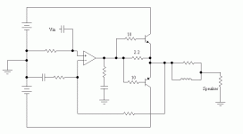
Why the 220nF caps on the chips power pins?
Can you use the chips mute circuit that way, or isnt it better just to omit the 22k resistor at the pin 8 completely (in this kind of circuit)?
This is an excellent point. The power chip supply pins are signal pins in this app, and the heavy filtering there can explain the shoot-through. Remove them, or move them to the power connections, but not on the chip pins!
Jan
Thanks to jan.didden for pointing out the 'shoot through' behaviour. Initially when I tested with LM3886 (pre-soldered board) it had 100uF capacitors in DC rail which I believe caused this issue. Most chip-amp pre-soldered boards have these caps next to DC input. I didn't know it would give a problem except for a switch on 'brr' noise powering on.
The LM3876 XY pcb with custom soldered 220nF in DC rail didn't cause it. No switch on noise - completely silent.
Left LM3876 vs. Right LM3886

palstanturhin in many TDA2030 \ LM1875 chips + power rail transistors topology there is a 100nF to 220nF cap connected in-between the transistor bases or chip +rail to -rail for high frequency stability. I added 220nF power supply decoupling caps from rails to ground too. Am planning to reduce these to 100nF.
If you wish use LM3875 & discard the mute section parts. The basis of my experiment was XY LM3886 pcb. As jan.didden suggested will move the mute section input before 2SC5200 in the -ve rail.
The LM3876 XY pcb with custom soldered 220nF in DC rail didn't cause it. No switch on noise - completely silent.
Left LM3876 vs. Right LM3886
palstanturhin in many TDA2030 \ LM1875 chips + power rail transistors topology there is a 100nF to 220nF cap connected in-between the transistor bases or chip +rail to -rail for high frequency stability. I added 220nF power supply decoupling caps from rails to ground too. Am planning to reduce these to 100nF.
If you wish use LM3875 & discard the mute section parts. The basis of my experiment was XY LM3886 pcb. As jan.didden suggested will move the mute section input before 2SC5200 in the -ve rail.
Last edited:
Thanks to jan.didden for pointing out the 'shoot through' behaviour. Initially when I tested with LM3886 (pre-soldered board) it had 100uF capacitors in DC rail which I believe caused this issue. Most chip-amp pre-soldered boards have these caps next to DC input. I didn't know it would give a problem except for a switch on 'brr' noise powering on.
The LM3876 XY pcb with custom soldered 220nF in DC rail didn't cause it. No switch on noise - completely silent.
Left LM3876 vs. Right LM3886
palstanturhin in many TDA2030 \ LM1875 chips + power rail transistors topology there is a 100nF to 220nF cap connected in-between the transistor bases or chip +rail to -rail for high frequency stability. I added 220nF power supply decoupling caps from rails to ground too. Am planning to reduce these to 100nF.
If you wish use LM3875 & discard the mute section parts. The basis of my experiment was XY LM3886 pcb. As jan.didden suggested will move the mute section input before 2SC5200 in the -ve rail.
Unless you have some other power supply caps located VERY close to where the power supply wires connect to the XY board the 220nF caps are WAY too low in capacitance to supply the LM3886 with local charge reserve and to bypass the supplies. It was recently brought up in another thread in this forum that the 100uF value typically supplied on the XY board is actually too small of a value for local bypassing of the LM3886 and 470uF is the min value recommended in the datasheet by National Semi. You could solder on a pair of 470uF or larger caps at the terminal pins where the PS wires enter the board and keep the 220nF caps for additional bypassing purposes.
CharlieLaub, thanks. I have modified the circuit by adding 2x 1000uF decoupling caps at the rails before the transistors.
Additional bypass caps reduced to 100nF. Added 330pF at the input. Moved mute circuit directly to -ve rail increasing the resistor to 100k for added delay.
Optional low forward drop D1 & D2 3A diodes could be added while using as Subwoofer amp to control back EMF = better damping ? It could add distortion when used as a full range amp.

Above schematic entails a new PCB design. I have had a local designer manufacture a PCB before. The purpose was to design a monoblock by mounting a class D TDA7498MV amplifier & a 24v SMPS (both bought from Aliexpress) on a base PCB serving as a motherboard with 6db crossover network.
Additional bypass caps reduced to 100nF. Added 330pF at the input. Moved mute circuit directly to -ve rail increasing the resistor to 100k for added delay.
Optional low forward drop D1 & D2 3A diodes could be added while using as Subwoofer amp to control back EMF = better damping ? It could add distortion when used as a full range amp.
Above schematic entails a new PCB design. I have had a local designer manufacture a PCB before. The purpose was to design a monoblock by mounting a class D TDA7498MV amplifier & a 24v SMPS (both bought from Aliexpress) on a base PCB serving as a motherboard with 6db crossover network.
Last edited:

Penjo,
just attach your pics.
It is the preferred method of this Forum.
There is even a Thread explaining to Newbies how to do it.
How to attach images to your posts.
just attach your pics.
It is the preferred method of this Forum.
There is even a Thread explaining to Newbies how to do it.
How to attach images to your posts.
Ok. For TDA7498MV add-on board I have attached the pictures in the below link:
Ebay cheap TDA7498 boards
Locking the thread after few minutes doesn't make it easy to revise technical errors. With an external link of an uploaded image, it can be deleted to avoid confusion.
Ebay cheap TDA7498 boards
Locking the thread after few minutes doesn't make it easy to revise technical errors. With an external link of an uploaded image, it can be deleted to avoid confusion.
Last edited:
- Status
- This old topic is closed. If you want to reopen this topic, contact a moderator using the "Report Post" button.
- Home
- Amplifiers
- Chip Amps
- LM3886 + output transistor