Hi
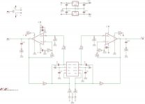
I made a new layout from the schematic donated by Russ some time ago.
It is very similar to the original although a little bit more compact and most important change is proberly the "singel" supply instead if separate supply to each LM3886.
Note. R15, R16 is going to be changed to SMD to make them fit behind the LM3886chip..
U3 is a THS4131 and not an ordinary OpAmp.
100uF decoupling caps will be place directly on the supplypins of
the LM3886
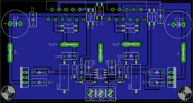
I tried an double layer version but did,nt get it to work.. major distortion and all kinds of funny noises.. So now i,m trying this version with a groundplane.. (almost a copy of Russ working prototype)
I,m looking for some help spotting any errors..
Thanx.
/JZ
I made a new layout from the schematic donated by Russ some time ago.
It is very similar to the original although a little bit more compact and most important change is proberly the "singel" supply instead if separate supply to each LM3886.
Note. R15, R16 is going to be changed to SMD to make them fit behind the LM3886chip..
U3 is a THS4131 and not an ordinary OpAmp.
100uF decoupling caps will be place directly on the supplypins of
the LM3886
I tried an double layer version but did,nt get it to work.. major distortion and all kinds of funny noises.. So now i,m trying this version with a groundplane.. (almost a copy of Russ working prototype)
I,m looking for some help spotting any errors..
Thanx.
/JZ
zei said:100uF decoupling caps will be place directly on the supplypins
That would be 100 nF not µF. C2 and C3 look to be that size already.
R15 and R16 seem very small. They should be smaller than (|Vee|-2,6)/0,0005, but not that much.
Are you aware that ground planes can also become antennas? And are you aware that neighboring traces and planes form capacitors? I recommend to look into National's reference designs to get a feeling for layout techniques.
More than 1/4 W should not be necessary for the Zobel resistors. If that is too small, it is probably due to a severe (layout-induced?) oscillation problem.
Thanx for the input Pacificblue.
You are correct about the caps. Thanx for the heads up.")
This i don,t understand. Care to explain ?
I,m aware of the issues that can happen with groundplanes however this cirquit has been tested with groundplane with successful result (Not messured though)
Zobel wont be used so i guess i can remove it.. (it was there on the original so i draw it in)
My main concern is the fact that the 2 LM3886 are sharing supply traces instead of having a separate trace for - +V to each LM3886 chip.
Is this a problem generaly?
Also i would be happy if someone can spot any obvious flaws or errors in the layout.
Thanx!
You are correct about the caps. Thanx for the heads up.
R15 and R16 seem very small. They should be smaller than (|Vee|-2,6)/0,0005, but not that much.
This i don,t understand. Care to explain ?
I,m aware of the issues that can happen with groundplanes however this cirquit has been tested with groundplane with successful result (Not messured though)
Zobel wont be used so i guess i can remove it.. (it was there on the original so i draw it in)
My main concern is the fact that the 2 LM3886 are sharing supply traces instead of having a separate trace for - +V to each LM3886 chip.
Is this a problem generaly?
Also i would be happy if someone can spot any obvious flaws or errors in the layout.
Thanx!
The bigger the resistor, the higher is the voltage threshold, where the muting current is reached. Clicks and pops happen, while the power supply is charging/discharging. Without a delay the best thing you can do to suppress those noises is to set the treshold as high as possible, just below the lowest voltage you can get on the V- rail.zei said:This i don,t understand. Care to explain ?
With a ground plane or with that ground plane?zei said:I,m aware of the issues that can happen with groundplanes however this cirquit has been tested with groundplane with successful result (Not messured though)
Courageous. Especially without proper bandwidth limiting and after your experience with the other PCB.zei said:Zobel wont be used
It could become a problem, if the traces are too narrow. The same goes for -V and the output trace, which are the ones, where most current will flow. How much current will flow there? Let me try an example. Your bridged amp will drive an 8 Ohm speaker with ±24 V rails. That leads to Ipk ~5,16 A, Ieff ~3,6 A per IC. Assume that the worst case headroom (MTV) is only 10 dB, then that leads to ~1 A per IC and ~2 A for the speaker traces. With 35 µm copper the -V and +V traces should be ~0,4 mm wide. The speaker traces ~0,9 mm. The wider, the better. That will be a challenge on a single-sided PCB.zei said:
My main concern is the fact that the 2 LM3886 are sharing supply traces instead of having a separate trace for - +V to each LM3886 chip.
Is this a problem generaly?
That is difficult. There are layout techniques you should follow. You didn't, but that does not necessarily mean the PCB won't work. On the other hand, if it doesn't, the layout could be one of the reasons (other than the combination of a fast control amplifier with a slow follower, which makes the combination prone to loop oscillations). Did you ever find out, why your other PCB didn't work? If you did, you could avoid to repeat the same mistakes again.zei said:Also i would be happy if someone can spot any obvious flaws or errors in the layout.
Here are some of the layout techniques you didn't follow.
- avoid right angled traces
- maintain a distance between neighboring traces and planes to keep capacity and inductive coupling low
- avoid closed loops in a ground plane
- place the ground connections of the big smoothing capacitors as close to each other as possible
- keep traces as short as possible
- don't fill too narrow spaces with the ground plane, e. g. below R7
- separate the ground into different paths, e. g. C7, C10 and the Zobels should have a return path separate from input ground and feedback loop ground
How about splitting this project into several PCBs? You could design one for an LM3886 and use it twice. Then design another one for the differential amplifier. That makes each design easier and gives you the opportunity to use at least the LM3886 PCBs later for another application, e. g. a "normal" bridged amp.
Hi Pacificblue
First, Thank you very much for your time.
(even if you answers make me feel more stupid for every time i read them )
)
About the groundplane, You are right to question this groundplane since it has.nt been tested with this groundplane.. But as you say, a groundplane works..
I,ll also reconsider the Zobel.. At least it wont do any harm to have the option..
I,ll take your hints and try to implement them as i understand them and also read the datascheets to get some tips.
Splitting it into severeal PCB,s is not an option at this point.
I already had a successful amp with Russ original singlesided layout (With groundplane) so i think i can make one again? With your help ofcourse You might ask why not use that same layout again? Answer would be.. learn to make your own layout.. and also make a bit smaller PCB to fit my chassi.
Oh i forgot, I never found out what was wrong with that former doublesided layout My mistake was proberly to not ask for help here first..
Thanx again.
/JZ
First, Thank you very much for your time.
(even if you answers make me feel more stupid for every time i read them
)About the groundplane, You are right to question this groundplane since it has.nt been tested with this groundplane..
But as you say, a groundplane works..I,ll also reconsider the Zobel.. At least it wont do any harm to have the option..
I,ll take your hints and try to implement them as i understand them and also read the datascheets to get some tips.
Splitting it into severeal PCB,s is not an option at this point.
I already had a successful amp with Russ original singlesided layout (With groundplane) so i think i can make one again? With your help ofcourse
You might ask why not use that same layout again? Answer would be.. learn to make your own layout.. and also make a bit smaller PCB to fit my chassi. Oh i forgot, I never found out what was wrong with that former doublesided layout
My mistake was proberly to not ask for help here first.. Thanx again.
/JZ
That is not their purpose.zei said:you answers make me feel more stupid for every time i read them
The question is, if the groundplane is there for a purpose other than good looks.zei said:I already had a successful amp with Russ original singlesided layout (With groundplane) so i think i can make one again?
A groundplane is not a bad thing, if you know how to use it. It can be used for shielding. In SMD applications it serves as heatsink for certain components. It provides a low resistance due to its width. It brings inductance down, and in a multi-layered PCB it provides you with short paths to ground, wherever you need them.
If I may recommend, learn the theory first. Then start with simple layouts and move towards more complex ones, as you achieve reliable operation.zei said:You might ask why not use that same layout again? Answer would be.. learn to make your own layout.
It seems as if Russ White had stopped support for this application.
- Status
- This old topic is closed. If you want to reopen this topic, contact a moderator using the "Report Post" button.
- Home
- Amplifiers
- Chip Amps
- TwistedX