don't apologise. No question is dumb.Sorry for what may be a particularly dumb question
This is a very good question.
What will the circuit try to do if the 3886 part enters mute mode?
Could the opamp survive this loading. Could it be operated outside of specification.
Will the 3886 mute function work as a mute when it is operated as a current source?
Yep, just look at the datasheet for the "mute" pin. It should be tied to -v through a 33k res or so. Just place a switch in there, so when it is "open", it will get muted.Folks:
Sorry for what may be a particularly dumb question, but is there a simple way to implement a mute function with the MyRef RevC?
Thank you,
Scott
mmmmm something about it comes to my mind. Something about being nested in the LM318 feedback loop and the mute function causing some instabilities.I may be mistaken, but I think Mauro originally stated that the mute function could NOT be used in this implementation...
Anybody out there with better memory?
What will the circuit try to do if the 3886 part enters mute mode?
Could the opamp survive this loading. Could it be operated outside of specification.
Will the 3886 mute function work as a mute when it is operated as a current source?
look at the datasheet for the "mute" pin. ............... Just place a switch in there, so when it is "open", it will get muted.
Regi,Something about being nested in the LM318 feedback loop and the mute function causing some instabilities.
do you read?
Read again the expanded three questions following SRMcGee post.
My apologies Andrew, I was at work, where the forum is seen like a crap. Login doesnt work well, website doesnt reload properly...I couldnt read your post.
Now I understand why it cannot be implemented, closer to what I had in mind. Thank you.
Sorry for that again, regards
Regi
Now I understand why it cannot be implemented, closer to what I had in mind. Thank you.
Sorry for that again, regards
Regi
Folks:
Okay, since it appears that I cannot exploit the mute function on the MyRef RevC LM3886, perhaps a relay can be used. Does it make any sonic difference where a "mute" relay is used in the circuit? This project involves a Pedja Rogic buffer, Lightspeed attenuator and the MyRef RevC, and the relay could be placed before or after any of these stages.
Regards,
Scott
Hi,
you could place an input mute activated by loss of mains power on any of the inputs.
I would be tempted to put one on the front end of MyRevC and also put one on the input to the pre-amp. But only if the source can drive the muted circuit without damage.
Have you read the threads talking about the LDRs and what happens when they are powered down?
As an aside.
The same MyRevC input muting relay could also be activated on detection of excessive output DC. Just in case it is a preceding source that has gone faulty.
Last edited:
Am I reading right? taking output to ground? that means a shortcircuit, an easy way to destroy the output stage. You may wanted to say a different thing or I am reading incorrectly.it would be better to take output to ground via relay.
The disadvantage of this method is that the audio signal passes across the relay contacts.
Depends on how good the relay is. So might sound better by just shorting the output to ground as you suggested.
I havent suggested anything new, is the same DC protection circuit onboard designed by Mauro. I am just putting a switch to force the relay to disconnect the speaker ground, thus disconnecting the speaker. No mods, no desoldering or cutting traces, just soldering two points for the switch.
If we are already passing the signal through a relay, why adding another one? Why not taking advantage of the one already implemented? In fact, I am only implementing the original idea you had about the DC protection circuit, Andrew.
Any more elegant solution out there? Any drawback?
BTW, I have a question about the DC protection. I wonder that, being the relay a mechanical device, it has a far higher response time than electronic devices. So, if DC current starts to flow on the outputs, a short space of time is there between the DC current flowing and the relay opening the circuit. So DC current will reach the speaker.
Last edited:
The output RCA hot pin to ground using the relay contact.
The third relay contact has the buffer output which is now unloaded, or has a dummy 1M0 load for this situation.
I wonder if the location of the mute is causing confusion.
I was referring to a mute on the output of the source. Are you referring to a speaker disconnect relay?
The third relay contact has the buffer output which is now unloaded, or has a dummy 1M0 load for this situation.
I wonder if the location of the mute is causing confusion.
I was referring to a mute on the output of the source. Are you referring to a speaker disconnect relay?
Last edited:
I think you mean RCA IN, not OUT. Myref doesnt have any RCA out.
So for this solution, we will need to add some way to supply that second relay. Or we could tap it from the myref board and regulate it to the desired voltage using another board for the regulator. Then add a switch to control it.
So in the end, we will have the signal passing through 2 relays, using more space and spending more money.
IMHO, it doesnt worth the effort. IMHO, I would go the other route. But you are a clever guy. If you go this approach is because there may be another reason I dont know about.
Regards,
Regi
Sorry, only just read this post.
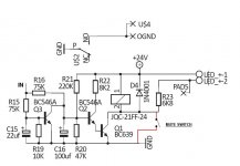
Why not forcing the protection relay to kick in? I have added a switch to the MyRef_C protection circuit schematic. Anybody see anything wrong with that?
QUOTE]
Am I being a bit dumb here but ...
The switch you propose causes the relay to energise (and kick in). But for mute don't we want to de-energise the relay?
Would putting a switch across R20 have the desired effect?
Cheers
Geoff
You are right, Geoff, you have to cut the current. I thought about that when you asked me by PM, but because nobody got interested I didn't concern.
Maybe the way you propose across R20 will work, I don't know. Someone knowing more about transistors could enlight us.
What we could do is placing the switch between the lower leg of Q1 and ground. You will only need to not solder that leg to the pad, and solder to a wire instead. Take it to the switch, and the connect the other end of the switch to the pad.
That WILL WORK
I wonder if the location of the mute is causing confusion.
I was referring to a mute on the output of the source. Are you referring to a speaker disconnect relay?
I did mean RCA out.I think you mean RCA IN, not OUT. Myref doesnt have any RCA out.
see my earlier posting.
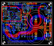
MyRef Version 1.3 layout
Not sure if this is the right thread to post this at, but it's not directly related to the MyRef build thread, so I decided to post it here instead.
Using the Twisted Pear Version 1.2 PCB layout posted here by Russ White in 2008 as the starting point, I made a lot of incremental improvements to the layout, now at Version 1.3. The changes are mainly in the following aspects:
1. Allows the use of larger-dimensioned electrolytics at several locations. This is particularly important for C1, C2, C3, C8 and C9.
2. Allows the use of a larger dimensioned input cap C13.
3. Allows the use of larger-dimensioned resistors at various locations, including R5, R6, R7, R8, R9, R10, R11, R12 and R13.
3. Improves placement of several components, notably in the region around IC1 (LM318). These include C6, C11, ZD1, ZD2 and the ground and power routing related to these. C19 and C20 have been dropped.
4. Improved ground and power routing at several locations, including separate star grounds for the power and LM318 sections.
5. Improved isolation of the signal ground plane from the chipamp power traces.
6. Numerous minor improvements in placement and signal routing in the small-signal input and LM318 compensation areas.
The schematic is exactly the same as before, with the same parts designations as Version 1.2 - so all the existing BoMs should work without modification, on the Version 1.3 layout as well. However, the board will be physically larger than the Version 1.2 board, which may be an issue with existing case/cabinet mounts and stand-offs.
Here's an outline of the layout, exported from Eagle. If there are any other changes/modifications that are considered desirable, feel free to post a request in this thread. I can't guarantee that I will implement it in this version, but it may make its way into future versions.
Attachments
- Home
- Amplifiers
- Chip Amps
- The new "My Ref" Rev C thread