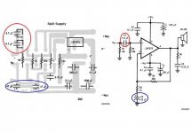
here is the example application for the LM1875 from the nat. semi. datasheet.
my question is regarding a few differences between this and example applications of lower power op amps in a typical non-inverting amplifier schematic (an example is either the CMOY pocket headphone amp or on the wikipedia page for operational amplifier applications for non-inverting amplifier schematic).
1) typically with headphone amps and general low power non-inverting amp. setups i see that there is no C2 capacitor as in the above schematic for the LM1875 and instead R3 goes directly to ground. what purpose does C2 serve?
2) what does the R5/C5 on the output pin, parallel to the speaker output, do?
3) i assume that the C1/R2 is for removing DC bias, and aside from a slight change in the corner frequency, moving to C1=0.47uF and R2=100KOhm, what implications/impact does this have on the overall design?
thank you,
christopher abad
An externally hosted image should be here but it was not working when we last tested it.
my question is regarding a few differences between this and example applications of lower power op amps in a typical non-inverting amplifier schematic (an example is either the CMOY pocket headphone amp or on the wikipedia page for operational amplifier applications for non-inverting amplifier schematic).
1) typically with headphone amps and general low power non-inverting amp. setups i see that there is no C2 capacitor as in the above schematic for the LM1875 and instead R3 goes directly to ground. what purpose does C2 serve?
2) what does the R5/C5 on the output pin, parallel to the speaker output, do?
3) i assume that the C1/R2 is for removing DC bias, and aside from a slight change in the corner frequency, moving to C1=0.47uF and R2=100KOhm, what implications/impact does this have on the overall design?
thank you,
christopher abad
Hi,
These are some very basic questions.
C2 will shunt DC in the feedback loop to ground, therefore it will not be amplified. This should be retained if you value your speakers/headphones.
R5/C5 is a Zobel. It is important for amp stability and should be retained. It has no effect on sound quality.
C1 blocks DC on input and with R2 form the input filter. There's a formula, but I'm too lazy to look for it but suffice to say that the values in the ap note are good ones.
(Ci + Ri) and Rf form a voltage divider to adjust how much of the output signal is fed back to the inverted input as correcting signal.
The lower the frequency the higher Ci's impedance in Ohm. That means more voltage drops across Ci + Ri and less across Rf. In other words the lower the frequency, the lower the feedback voltage at the inverting input and the lower the gain. The lowest possible gain is unity below the frequency where Ci + Ri = Rf, in this example around 0,38 Hz.
F(-3) for this filter is around 6,55 Hz, where the gain is halved. Not where Ci = Ri, which would be around 7,23 Hz.
Attached is an image of the example schematic and layout from the LM1875 datasheet.
I noticed on the layout C1 and C2 are both shown as pairs of capacitors with opposing polarities. To me this looks like a mistake, but it is National's datasheet. Are the polarities shown on the layout correct?
I noticed on the layout C1 and C2 are both shown as pairs of capacitors with opposing polarities. To me this looks like a mistake, but it is National's datasheet. Are the polarities shown on the layout correct?
Attachments
Yes. By connecting two polarized capacitors in series back-to-back you create a non-polarized capacitor with half the capacitance. They work, as if each of them was by-passed by a diode, so each of them is active for one half of the sine-wave. This design is already old, and when it was made non-polarized capacitors were not as readily available and cheap as they are today. Therefore two polarized types were chosen instead.
If you want to build this amplifier you could (should) replace those two polarized caps with a single non-polarized as per the schematic, e. g. an MKP capacitor to achieve a better sonic performance.
If you want to build this amplifier you could (should) replace those two polarized caps with a single non-polarized as per the schematic, e. g. an MKP capacitor to achieve a better sonic performance.
Hi,
the National schematic although correct needs a little tweaking to get the best out of it.
The input has one (high pass) filter on it. It needs two. A low pass filter should be added to attenuate RF interference.
This can be a low inductance capacitor fitted in parallel to R2, an MKP 330pF to 1nF does the job.
It needs a resistor to complete the filter.
Add the resistor in series with C1, a value of 470r to 1k0 will do.
Use an MKT, MKS, MKP for C1 rather than a cheap electrolytic.
I would change the value of R2 to 47k, but that's just a personal choice to suit the way I like the bass response of the input filters.
The value of C2 is quite simply wrong. It must be much bigger than 22uF.
C2 >= {1.4 * C1 * R2 / R3}
if R2=22k then C2>=68uF.
if R2=47k then C2>=146uF.
Use a good quality polarised electrolytic here.
Add a pair of inverse parallel diodes across the electrolytic pins as well. This is to prevent the capacitor going over voltage if the amp decides to play up/produce DC on the output.
Consider adding a low value MKP across the electrolytic pins. But be prepared to remove it if you don't like the effect it has on the sound.
You should also consider adding the output inductor//resistor that National show on the datasheet.
C3 & C4 must be located on or very close (5mm) to the chip's power pins. The common leg between them must be very short (<20mm)
Do not connect C2 to a common ground.
Connect R1, R2 and C2 to a dedicated Signal Ground that is taken to the ground of the input socket. Connect the input socket to the main Audio Ground that also connects the Speaker Return.
Finally, complete the RF attenuation by adding a 47pF directly across the input socket, +IN to -IN (tip to barrel)
Everyone has explaind what the components do in each case.
let me just add to it a bit differently .
C1 blocks dc at the input. It also defines the -3dB point for LF in conjunction with R2. ( C= 1/ ( 2*pi*F*R2) Where F is the desired frequency where the response drops to -3dB . Usually much lower than 20 Hz so that you get very little phase shift ( maybe 2 Hz or 4 Hz ).
R1 makes a dc path to ground for C1 so that the input terminal is at zero potential. Otherwise after power on if you plug in an input you will get a bang at the output when C1 gets charged up. May or may not result in some damage. C1's input terminal must be kept at zero potential to avoid a dc impulse at the output when you plug something in after power up.
C2 is there to provide an ac path to ground and block the dc path to ground ( in effect open circuit for dc).
C2 looks like an open circuit to dc ( if it's a good capacitor !). So dc gain of the circuit is 1. So a 10mV error at the input should look like a 10 mV at the output...very good. If you short C2 ( no C2 ) then dc gain is equal to ac gain ( here 20/1 + 1 = 21) . So 10 mV will now be 210 mV at the output. Not good but will not cause any physical damage to the speaker. It will cause a dc offset to the cone poosition which is not good for several reasons. If the dc input offset is bad ( higher) it can be a real problem!
R5/C5 is the Zobel that is there to nullify the effect of speaker inductance. On some systems it will cause oscillations if it's not present. But on others it will not seem to have any effect. If the application diagram shows it , you better use it. While 10 ohms and 0.1uF is very commonly seen you will sometimes find different values on some circuits . On simulation you can clearly see how it effects square wave reproduction.
R2 also carries the input stage base current. So larger values of R2 will cause a bigger dc drop on it and hence increase input offset voltage and hence the output offset voltage.
With C2 in place the effect might not be too bad with a R2 of 100K ohms. But if you plan on eliminating C2 you will have to think of keeping R2 and the feedback resistor values ( R4/R3) low to reduce dc the offset voltage.
Just another way of repeating what all the others have said!
")
let me just add to it a bit differently .
C1 blocks dc at the input. It also defines the -3dB point for LF in conjunction with R2. ( C= 1/ ( 2*pi*F*R2) Where F is the desired frequency where the response drops to -3dB . Usually much lower than 20 Hz so that you get very little phase shift ( maybe 2 Hz or 4 Hz ).
R1 makes a dc path to ground for C1 so that the input terminal is at zero potential. Otherwise after power on if you plug in an input you will get a bang at the output when C1 gets charged up. May or may not result in some damage. C1's input terminal must be kept at zero potential to avoid a dc impulse at the output when you plug something in after power up.
C2 is there to provide an ac path to ground and block the dc path to ground ( in effect open circuit for dc).
C2 looks like an open circuit to dc ( if it's a good capacitor !). So dc gain of the circuit is 1. So a 10mV error at the input should look like a 10 mV at the output...very good. If you short C2 ( no C2 ) then dc gain is equal to ac gain ( here 20/1 + 1 = 21) . So 10 mV will now be 210 mV at the output. Not good but will not cause any physical damage to the speaker. It will cause a dc offset to the cone poosition which is not good for several reasons. If the dc input offset is bad ( higher) it can be a real problem!
R5/C5 is the Zobel that is there to nullify the effect of speaker inductance. On some systems it will cause oscillations if it's not present. But on others it will not seem to have any effect. If the application diagram shows it , you better use it. While 10 ohms and 0.1uF is very commonly seen you will sometimes find different values on some circuits . On simulation you can clearly see how it effects square wave reproduction.
R2 also carries the input stage base current. So larger values of R2 will cause a bigger dc drop on it and hence increase input offset voltage and hence the output offset voltage.
With C2 in place the effect might not be too bad with a R2 of 100K ohms. But if you plan on eliminating C2 you will have to think of keeping R2 and the feedback resistor values ( R4/R3) low to reduce dc the offset voltage.
Just another way of repeating what all the others have said!
AndrewT said:Hi,
the National schematic although correct needs a little tweaking to get the best out of
The value of C2 is quite simply wrong. It must be much bigger than 22uF.
C2 >= {1.4 * C1 * R2 / R3}
if R2=22k then C2>=68uF.
if R2=47k then C2>=146uF.
Use a good quality polarised electrolytic here.
Add a pair of inverse parallel diodes across the electrolytic pins as well. This is to prevent the capacitor going over voltage if the amp decides to play up/produce DC on the output.
Consider adding a low value MKP across the electrolytic pins. But be prepared to remove it if you don't like the effect it has on the sound.
What is the largest voltage C2 might see??Most of the PCB's follow the data sheet value at 22uf 25v. Larger values at 25v are'nt going to fit.. I think you stated previously that it should be 10x larger!!!
Hi,
with the diode protection the cap can never see more than 1V of either polarity across it.
If it is sized correctly it should never have any AC voltage across it that can be measured on a standard 200mV DMM.
It is common to use electrolytics between 6V and 16V for this duty.
with the diode protection the cap can never see more than 1V of either polarity across it.
If it is sized correctly it should never have any AC voltage across it that can be measured on a standard 200mV DMM.
It is common to use electrolytics between 6V and 16V for this duty.
it depends on the filter at the input. 10times larger (=220uF) applied for that case only.that it should be 10x larger!!!
the input filters set the users bandwidth.digi01 said:i think c2 value will affect opamp bandwidth,then involved with gain.
but opamp is not equal to poweramp
C2 sets the DC gain to 1 just the same whether it's a power amp or a chipamp or an opamp.
Thank you all for lending your expertise, your explanations are helpful.
AndrewT, I'll be taking some (maybe all) of your advice. I do see the inductor//resistor on the LM3875 and LM3886 data sheets for the single supply circuits, at least as optional components.
I did find this thread on the subject, so I'll be doing some reading:
http://www.diyaudio.com/forums/showthread.php?threadid=125679
I have 10 of these chips. My plan is a pair of mono blocks and some experimenting.
AndrewT said:You should also consider adding the output inductor//resistor that National show on the datasheet.
AndrewT, I'll be taking some (maybe all) of your advice. I do see the inductor//resistor on the LM3875 and LM3886 data sheets for the single supply circuits, at least as optional components.
I did find this thread on the subject, so I'll be doing some reading:
http://www.diyaudio.com/forums/showthread.php?threadid=125679
I have 10 of these chips. My plan is a pair of mono blocks and some experimenting.
The value of C2 is quite simply wrong. It must be much bigger than 22uF.
C2 >= {1.4 * C1 * R2 / R3}
if R2=22k then C2>=68uF.
if R2=47k then C2>=146uF.
Use a good quality polarised electrolytic here.
Add a pair of inverse parallel diodes across the electrolytic pins as well. This is to prevent the capacitor going over voltage if the amp decides to play up/produce DC on the output.
Consider adding a low value MKP across the electrolytic pins. But be prepared to remove it if you don't like the effect it has on the sound.
Hi Andrew
I would like to understand that eq you mention for C2 calculation. Could you explain it to me? What's the point for C2 to be exactly that value? There's no BW compromise for C2 to be 22, 68, 100 or 150uF I guess, at least in AF.
I think i will use R2=33K and C2=100uF, because I already have them, lol.
Thank you, you're very helpful.
Finally, complete the RF attenuation by adding a 47pF directly across the input socket, +IN to -IN (tip to barrel)
Could I ask how the value for this capacitor is determined? I have 220pF in this position, is it too much?

Thanks.
- Status
- This old topic is closed. If you want to reopen this topic, contact a moderator using the "Report Post" button.
- Home
- Amplifiers
- Chip Amps
- LM1875 and questions regarding the example application in the datasheet