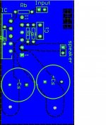
Hi can anyone pls have a look at a preliminary PCB design for lm3886. It is a the bog standard design from the datasheet minus mute cap and switch, and no input pot. Its still rough but i want to sort issues out now!
I am unsure whether the supply and speaker ground should be connected to chip and signal ground as it is now. ie should there be only one ground.
The intention of this board is for application in a tri-amped system ie. 3-way active crossover with separate amps for tweeter, mid and woofer.
I am also unsure of decoupling cap sizes-planned is for 220uF in parallel with 100uF (not whats on the PCB-will still sort that out when im sure). The PS (external) contains quite a staunch cap network already.
Please point out any obvious mistakes or bad layout practice. any suggestions or questions....?
your help would be appreciated
Thanks Chris
13814044 said:Please point out any obvious mistakes
You haven't posted a schematic or image of the layout...
w
Andrew
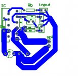
I'v had another look.
Do you feel all the optional components are necessary, especially wondering about the L-R network on the speaker out-is this often a problem or only with exceptionally long speaker leads.
I'll definitely add Cf, Rf2, Rsn and Csn.
Do you think i should go to a 2-layer board, with the star ground on top.
Should i use the component values listed in fig 2 or can you recommend better?
Thanks
Chris
a few links can usually avoid the need to/complexity of going to 2layer.
Allow for all the components. Adding them after you've omitted them is at best untidy.
Long speaker leads are not the sole problem. It's a combination of inductance and capacitance and interference coming back in to the speaker terminals that must all be addressed and using a full Thiele network rather than just a Zobel or nothing is recommended.
I used to recommend fitting the Thiele at the speaker terminals, but having read a persuasive argument on the Forum, I am inclined to now try mounting the Zobel part close to the output stage, i.e. on the PCB.
Star ground the power side of the PCB.
Star ground the signal side of the PCB.
Allow for a link to interconnect them or to take them separately to a remote Audio Ground.
2-layer is not too much of a problem-PCBs cost me almost nothing. So I think ill go that route, I feel i can come up with a design with much shorter tracks and a more logical layout this way.
Is the ground pin on the lm3886 considered part of the power or signal side.
will have a look at the Thiele network and include all optional components.
Should I use the indicated values or can you recommend other
Is the ground pin on the lm3886 considered part of the power or signal side.
will have a look at the Thiele network and include all optional components.
Should I use the indicated values or can you recommend other
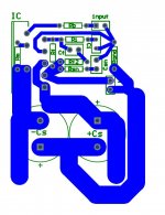
I'v fixed her.
Can anyone let me know if this design is any better. Single sided with all optional components (Zobel network will be placed at the speaker as recommended)
Should i keep the power and signal ground separate or as in the current layout-joined.( AndrewT recommended either)
as before I will sort out supply caps when this PCB gets a thumbs up- i just want you guys to approve it in principle.
Any input is appreciated as this is my first PCB
Thanks
Chris
Attachments
Move the Zobel return to the Power ground.
Break the trace between Power ground and Signal ground. Insert a pair of holes to tie these together with a link or resistor.
Where are the decoupling caps? 0u1F?
Remove pin2 & pin11 and maybe pin6.
Where is the RF attenuation?
You seem to have two extra components (R+C), that I don't recognise, from speaker to pin10.
Have another look at that other thread you could maybe share ideas.
Last thought.
Add alternative pin pitch for most or all of your caps. I just hate it when I can't find the correct pin pitch cap from stock but have plenty of the correct value and my usual suppliers don't do them either.
Hi Andrew
I'v made the annotations bigger so you can see whats what. I have all component indicated in the data sheet and they are labeled in the same way so it can be used as a key for interpreting my PCB.
Decoupling cap sizes have not been finalized-please advise. (I have 5*6 800uF on positive and negative supply rails located at the PS unit)
The extra components you refer to are Rf2 and C2 (fig 2-datasheet). I'm unsure of what part of the circuit is the RF attenuation-is it on the data sheet.
GNDs are now tied with res-should they still return to audio GND via separate wires?
Extra IC pins are gone.
Attachments
")
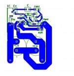
Hi
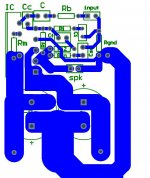
This is what it looks like now-removed Rb, added C and Cc.
Do i need to work on getting supply rails thicker-they're 5mm at their thickest areas.
any other suggestions on the basic layout? (I'll get to adding multiple footprints for the supply caps still.)
Again should i now still run separate GND wires the the audio ground
Thanks
Chris
Attachments
C and Rb should be in series for the input feed.
With the separated Signal and Power Grounds, you now have choices.
For a monobloc with transformer + PSU+Case+amplifier for one channel, connect SG to PG on the PCB, with either a link or low value resistor.
For a two channel amp with a common PSU, take all the signal and power grounds to a central Audio Ground (AG), but keep all the routes very short. This can be done with a centre tapped or dual secondary transformer and a single bridge rectifier.
For a two channel amp with separate PSUs, take each channel's SG & PG to their own AG and then connect each AG to Safety Earth with a pair of disconnecting networks. This requires dual bridge rectifiers for each channel and a dual secondary transformer.
Is this getting there yet?
I'll probably drill the holes for supply caps myself when i have them-I think theres enough room for experimentation (caps can be rotated slightly or shifted)
I definitely need all the flexibility i can get as the system will comprise of 6 or 8 amp modules with a single 1000VA toroidal.
3-way active crossover is already built from a kit
Attachments
- Status
- This old topic is closed. If you want to reopen this topic, contact a moderator using the "Report Post" button.
- Home
- Amplifiers
- Chip Amps
- lm3886 PCB