I made a few changes to my original PCB design for a small 1W stereo amplifier. I'm still pretty new at all of this, and I was hoping someone could point out some errors, if there are any, or just tell me how to improve my board. Pictures of both layers of the board are attached; please take a look. Thanks!
Attachments
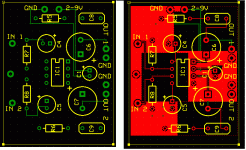
Well, thanks. My design has two layers (one layer has red tracks, and the other green) but the components will still all be mounted on one side, correct? Also, where exactly do I put that capacitor? And someone told me this specifically:
"You need to use star ground, the R6 ground which is part of the output filter should not share the same ground of the input ground. The input ground should be on its own trace run to the main GND point, same for the output. The power supply caps ground should also run to the GND without sharing with the input ground."
Can someone please explain to me what that means? I'll do some tweaking and repost my design, but I'm a bit confused.
capacitor should be placed as near as possible to IC and other pin is to be grounded.
As for second part regarding "star ground" this refers to grounding topology, you can find lot of info just google around "power supply grounding topolgies, or grounding topologies"
As for me I prefer the ground plane. I dont use star ground topology, but u ll find many supporters of the same, its upto individual which toplogy one wants to use.
- Status
- This old topic is closed. If you want to reopen this topic, contact a moderator using the "Report Post" button.
- Home
- Amplifiers
- Chip Amps
- First PCB Design Revised. Still looking for errors.