Sorry, I was not suggesting that you are daft at all. it is a matter of degrees as to the level of knowledge.
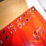
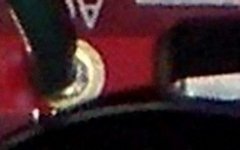
From the picture it looks as though you have no solder pad left at the point either ? This is why the solder is forming a ball around the leg of the diode.
As I suggested earlier yuo can get over the problem by scraping the lacquer off and connecting a wire to the leg with the good solder pad.
You have two of these boards to make a dual mono amp. For the time being you could use just one board and one tranny for both amps, unti you get the other sorted out, or have I just insulted you again ?!
Tripmaster said:I maybe daft...but not that daft ;}
I am having problems soldering the good contact.
As you can see from the photo I have sanded the copper contact.
The solder either forms a ball or sticks to the leg of the diode
Bend that leg straight up and join it the the available connection?
Gold contacts are big trouble unless you use gel flux. Its necessary to wipe that stuff off the soldering iron before each solder joint. A quick touch on some #0000 steel wool will remove the carbonized flux from the soldering iron.
I noticed that the solder has clumped. If there had been gel flux involved, that ball of solder would have been a beautiful shiny chrome color and the solder would also have covered the entire leg of that diode in sparkling clean mirror-shiny flux.
So, double-check your soldering materials.
Tripmaster said:Well I think I may be back in business. Well...at least until tested!
I used a surplus leg from another component to bridge the gap.
I purchase some new tips from Maplin today and they made all the difference
Thanks for your help.
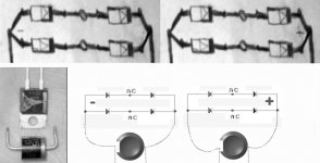
WOW!! That's not a bridge rectifier!!! The jumper shown in post #19 goes up parallel with the trace.
However, the jumper shown in post #26 goes over, horizontal, also parallel with the trace--its own trace, which is on the top side of the board. It doesn't go as shown in the photo of post #26 because that will make the transformer quite upset.
In post #26, its probable that, with flux, you can make that attachment from the top side of the board (where that trace is located) and not require a jumper.
See attached illustration for polarity in a dual-secondaries-supporting power supply, like yours.
Attachments
Questions:
Do you have a dual secondaries transformer (four ac output wires) or do you have a center tap transformer (three ac output) wires? I ask because the hookup is quite different.
Do you have gel flux painted onto the solder pads before attempting to solder? I ask, because gold pads will react, as shown in the photos above, whenever there's insuficient flux application prior to soldering.
For gold-doubleside boards, like yours, its necessary to get gel flux completely down the hole. I know its sticky (that's the point), but you can "push" the gel flux down the holes so that the solder follows it--[i[completely filling the holes with solder.[/i]
Do you have a desoldering iron, also called "solder sucker"? I ask because it can help prevent damage as shown in the photos above.
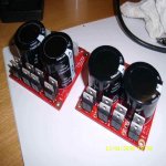
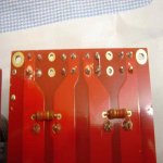
Here is a photograph of the component that's missing from the circuit boards pictured above.
Do you have a dual secondaries transformer (four ac output wires) or do you have a center tap transformer (three ac output) wires? I ask because the hookup is quite different.
Do you have gel flux painted onto the solder pads before attempting to solder? I ask, because gold pads will react, as shown in the photos above, whenever there's insuficient flux application prior to soldering.
For gold-doubleside boards, like yours, its necessary to get gel flux completely down the hole. I know its sticky (that's the point), but you can "push" the gel flux down the holes so that the solder follows it--[i[completely filling the holes with solder.[/i]
Do you have a desoldering iron, also called "solder sucker"? I ask because it can help prevent damage as shown in the photos above.
Here is a photograph of the component that's missing from the circuit boards pictured above.
Attachments
Tripmaster.It looks as though you have got it sorted.
In relation to the question regarding your transformer. The Clairtronic tranny's have dual secondary's which is how the Chipamp.com boards are configured.
If you were to use a centre tapped tranny you would need to modify the boards, (there are pictures on one of the threads on here of how to do it) but don't worry about something that is irrelevant.
danielwritesbac said:Here is a photograph of the component that's missing from the circuit boards pictured above.
That's not plumber's flux is it? Only use flux meant for electronics when soldering electronics. Kester RMA is a good liquid flux to use.
BWRX said:
That's not plumber's flux is it? Only use flux meant for electronics when soldering electronics. Kester RMA is a good liquid flux to use.
Hi Brian!! Thanks for the recommend.
The nasty sticky jar of stuff is Radio Shack flux. After the first use, I had to use a pipe wrench to open the lid--so plumber's tools were involved.
After it dried slightly, its so effective that its impossible to put the lid back on anyway (I put the lid on upside down now). Still, it makes all of the solder joints look like beautiful mirror shiny chrome color.
Is the Kester easier to remove?
The RS gel flux is impossible to remove from very tight pitch transistors. Otherwise, a half-hour's work with 99% alcohol and the toothbrush, can get 88% of it off the circuit board.
Anyway, I honestly believe that the gel flux will instantly tame those stubborn gold plate contacts, so you can use a safer low-heat soldering iron.
Edit: See picture. This is one of the wires from my transformer, soldered to that very same power supply board. It was soldered from the bottom, yet the hole is all the way full of shiny solder--from bottom to top with zero gaps.
Attachments
Hey, did you fix that short?
http://www.diyaudio.com/forums/showthread.php?postid=1483577#post1483577
is in regards to
http://www.diyaudio.com/forums/showthread.php?postid=1483199#post1483199
http://www.diyaudio.com/forums/showthread.php?postid=1483577#post1483577
is in regards to
http://www.diyaudio.com/forums/showthread.php?postid=1483199#post1483199
I'm breathing a sigh of relief that it wasn't plugged in this way.
http://www.diyaudio.com/forums/attachment.php?s=&postid=1483199&stamp=1208117707
http://www.diyaudio.com/forums/attachment.php?s=&postid=1483199&stamp=1208117707
Tripmaster said:I am beginning to regret naming this subject 'What a doofus!'
Every time I receive a notification email from the forum I am reminded of this fact!
I am receiving conflicting advice with regards to the the jumper pictured below.
Any other suggestions?
Remove that jumper and use the topside connections on the board. The traces relavant are on the top side anyway. So, that will help a lot.
EDIT: As shown in the photos, the traces are the lighter color red.
EDIT2: Hey, don't feel bad! My first experience with one of those supplies took a four hour "staring contest" between it and I. Finally, I visited On-Semi's website, marked the proper stripes on the diode, got the pencil and paper to sketch out the circuit, and checked it with the textbooks. . . all told, half a day's time.
- Status
- This old topic is closed. If you want to reopen this topic, contact a moderator using the "Report Post" button.
- Home
- Amplifiers
- Chip Amps
- What a doofus!