Hi folks. I'm splitting this question out from an entirely unrelated thread. Sorry to reopen an old wound, but the 'canonical' thread explaining why dual secondary/dual bridge has theoretically better noise performance than center-tap/single-bridge leaves me partially unfufilled.
The argument was considered more or less settled by the following post by Fred Dieckmann:
http://www.diyaudio.com/forums/showthread.php?postid=143874#post143874
...and past that was mostly people working out the implications. However, I have an implication question that wasn't explicitly explained. I don't want to argue-- I want to understand.
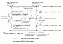
Fred's explanation does not address why and when slightly differing ground potentials at Vgnd3, Vgnd4, Vgnd5, etc in the top diagram matter in the slightest. I'm guessing an assumption that's obvious to him isn't obvious to me (or I'm assuming design givens he was not).
I assume in his diagrams that each amp submodule is connected to the power supply via a single ground return to one of the marked VgndN. If each submodule is self-contained (ie, if each submodule is handling an entire signal path from input through the amp to speaker output) and each of these sub-signal-paths are referenced to ground through a single return, why would the slightly different potentials at the Vgnds make any difference? For the whole signal path, input to output, the signal is referenced to the same ground.
I could see the point if, eg, there is an active preamp stage in addition to the amplifier, and each is being seperately grounded to the power supply. *There* your slight non-unity ground potential differences will cause trouble, as one part of the signal path is referenced to one ground, and another part of the same signal path is referenced to a slightly different ground.
Quoting Fred:
Is my interpretation above all Fred meant by that? If so, it doesn't seem like that's really all that much of a huge disadvantage to the single bridge design... You need to be aware and methodical about ground path with either topology. It's more 'if you do your ground topology wrong, single bridge will be noisier than dual bridge'.
(I can see this maaaaybe has a point in the chipamp.com kit where PG+ and PG- are being sent seperately and connected to opposite sides of a plane on the amp board... is there any advantage to that over bridging them on the PS board and sending a single ground? Keep all things equal, assume the same total amount of copper connecting ground...)
And, as this is an unregulated and [relatively] unfiltered supply, the debate is also ignoring the fact that there's plenty of hum on the rails anyway and we're relying heavily on the chipamp's high power supply rejection ratio (PSRR).
What am I missing? Or do I finally have it?
(BTW, I loved Fred's comment about the order of the ring terminals on a bolt affecting ground noise levels. Well yeah-- any mechanical connection will have a measurable resistance. Even solder joints have measurable resistance. Compared to copper, solder is a really crappy conductor.)
[edit: spelling, grammar, content, pants]
The argument was considered more or less settled by the following post by Fred Dieckmann:
http://www.diyaudio.com/forums/showthread.php?postid=143874#post143874
...and past that was mostly people working out the implications. However, I have an implication question that wasn't explicitly explained. I don't want to argue-- I want to understand.
Fred's explanation does not address why and when slightly differing ground potentials at Vgnd3, Vgnd4, Vgnd5, etc in the top diagram matter in the slightest. I'm guessing an assumption that's obvious to him isn't obvious to me (or I'm assuming design givens he was not).
I assume in his diagrams that each amp submodule is connected to the power supply via a single ground return to one of the marked VgndN. If each submodule is self-contained (ie, if each submodule is handling an entire signal path from input through the amp to speaker output) and each of these sub-signal-paths are referenced to ground through a single return, why would the slightly different potentials at the Vgnds make any difference? For the whole signal path, input to output, the signal is referenced to the same ground.
I could see the point if, eg, there is an active preamp stage in addition to the amplifier, and each is being seperately grounded to the power supply. *There* your slight non-unity ground potential differences will cause trouble, as one part of the signal path is referenced to one ground, and another part of the same signal path is referenced to a slightly different ground.
Quoting Fred:
Either method will work but the single brige requires much greater attention to the ground return path.
Is my interpretation above all Fred meant by that? If so, it doesn't seem like that's really all that much of a huge disadvantage to the single bridge design... You need to be aware and methodical about ground path with either topology. It's more 'if you do your ground topology wrong, single bridge will be noisier than dual bridge'.
(I can see this maaaaybe has a point in the chipamp.com kit where PG+ and PG- are being sent seperately and connected to opposite sides of a plane on the amp board... is there any advantage to that over bridging them on the PS board and sending a single ground? Keep all things equal, assume the same total amount of copper connecting ground...)
And, as this is an unregulated and [relatively] unfiltered supply, the debate is also ignoring the fact that there's plenty of hum on the rails anyway and we're relying heavily on the chipamp's high power supply rejection ratio (PSRR).
What am I missing? Or do I finally have it?
(BTW, I loved Fred's comment about the order of the ring terminals on a bolt affecting ground noise levels. Well yeah-- any mechanical connection will have a measurable resistance. Even solder joints have measurable resistance. Compared to copper, solder is a really crappy conductor.)
[edit: spelling, grammar, content, pants]
I only read Fred's post and looked at the diagram, but the diagram could use a little revising and clarification. The key difference between dual secondaries/bridges and a center tapped secondary with a single bridge is in how the supply caps are charged and how the ground is wired up to the amplifier modules.
I have more to write but I need to go to lunch")
I have more to write but I need to go to lunch
Well, yeah, I got that much I fully understand Fred's diagram, what I want to know about are the implications of that diagram on the rest of the system...
Eg, on a true single-channel monoblock with an electrically isolated input and a BrianGT 3886 chipamp module, Fred's diagram does not appear to lend any advantage whatsoever to the dual bridge.
For, eg, a stereo setup with two BrianGT boards, fully isolated inputs and a single ground path each back to the rectifier board, I still see no advantage in the dual bridge setup. The slightly different ground potentials do not affect the signal handling of the two boards as the boards do not 'see' each other in any sense.
I can see it could/would make a difference with non-isolated, especially unbalanced inputs, where even if the input grounds are handled carefully within the stereo amp, they're probably not isolated at the output device, then you have a ground loop potential (liklihood in fact). Then the dual bridge makes sense.
But that's very different from implying any sane high-end amp should use the dual bridge. Because in 'high end' setup (in my book), the inputs are balanced, and fully isolated/floating. There's no potential for a ground loop through them. A dual bridge here appears to offer nothing but higher component count. The concept of mitigating hum through power supply topology while still using ground-coupled unbalanced inputs strikes me as rearranging deck chairs on the Titanic.
Anyway, looking forward to more after lunch
I fully understand Fred's diagram, what I want to know about are the implications of that diagram on the rest of the system...Eg, on a true single-channel monoblock with an electrically isolated input and a BrianGT 3886 chipamp module, Fred's diagram does not appear to lend any advantage whatsoever to the dual bridge.
For, eg, a stereo setup with two BrianGT boards, fully isolated inputs and a single ground path each back to the rectifier board, I still see no advantage in the dual bridge setup. The slightly different ground potentials do not affect the signal handling of the two boards as the boards do not 'see' each other in any sense.
I can see it could/would make a difference with non-isolated, especially unbalanced inputs, where even if the input grounds are handled carefully within the stereo amp, they're probably not isolated at the output device, then you have a ground loop potential (liklihood in fact). Then the dual bridge makes sense.
But that's very different from implying any sane high-end amp should use the dual bridge. Because in 'high end' setup (in my book), the inputs are balanced, and fully isolated/floating. There's no potential for a ground loop through them. A dual bridge here appears to offer nothing but higher component count. The concept of mitigating hum through power supply topology while still using ground-coupled unbalanced inputs strikes me as rearranging deck chairs on the Titanic.
Anyway, looking forward to more after lunch
Ground loops are not the only potential problem. And we need to think in terms of dynamic (changing) ground voltages (not just DC and not just 100/120 Hz). You don't want your amp's signal input ground reference bouncing around, since the bouncing would then be summed into the input signal. And, actually, when dynamic ground-return currents cause any of the amplifier ground voltages to change, each is another form of feedback being added to the system, which can cause distortion, or even oscillation.
gootee said:Ground loops are not the only potential problem. And we need to think in terms of dynamic (changing) ground voltages (not just DC and not just 100/120 Hz). You don't want your amp's signal input ground reference bouncing around, since the bouncing would then be summed into the input signal.
Signal input only references ground if the input is unbalanced and non-isolated. Eg, the deckchairs/Titanic case. If you really care about hum/noise, the first thing you do is use a balanced/isolated input stages. If the inputs are galvanically isolated from the signal ground, noise on ground does not sum into anything.
gootee said:And, actually, when dynamic ground-return currents cause any of the amplifier ground voltages to change, it is another form of feedback being added to the system, which can cause distortion, or even oscillation.
In each amplifier subsystem, all they see is their own ground. Ground is always relative. They can 'bounce' relative to each other all they want, and it matters not an iota to the signal, because from the input stage all the way to the speaker, it is referenced to that same ground.
On the other hand, if ground is defined to be unity, then the noise 'shows up' on the V+/- rails instead. Either way, potential is changing across the rails/ground and that causes charge to move. I can see that affecting the amp, yes, but I'd assume if the PSRR is (typ) 120dB on a 3886, that applies equally to damping any supply feedback.
Also, that doesn't apply to the one amp/one supply case (you never said it did, just being explicit).
[edit: related question: do the chip amps typically push/pull through the ground, or is the ground treated as a low-current reference and the charge is moved through the V+/- rails?]
Actually, let me restate some of that last post more clearly...
A ground 'bouncing' is a relative thing. If all you can see is that ground, it doesn't really matter if it's moving around in relation to some other ground, because [ideally] the local ground potential is all you see. What matters, and what makes it non-ideal, is if current is flowing through that ground. That will cause point potentials along that ground path to differ, and within an amp subsystem, it's not physically possible for all atomic components in that subsystem's signal path to be referencing the exact same ground point.
So, it's not really a matter of relative potential, it's a matter of current generating nonuniform potentials. Let's define, then, a 'bouncy ground' to be a ground that has a noisy current flow.
Maximally isolated signal paths share only three points of coupling; ground, V+ and V-. Any current flowing to ground would have to be coming from the V+ or V- rails (as the inputs and outputs are fully isolated from one another, they cannot source/sink current from another input/output). In the typical chipamp, the only connections to V+ and V- are the chipamp chip itself.
So, the question boils down to, is the chipamp chip itself sourcing/dumping non-negligable current into and out of the ground, or is it too only using it as a reference and steering current through the rails? Given the very high PSRR, I'd say it's probably only using the ground as a reference....
Monty
Hi,
First, I'd say be careful about relying a power chip's PSRR to fix anything (unless you go full class-A and full bridge == clean rails by design). And the major problem is not PSU hum/buzz -- which, if some filtering is applied to it, seems to be rather benign in spectral content and will be PSR'd away --, rather the load current induced disturbance (which is halve-wave rectified stuff) is making the troubles and needs to be adressed with proper decoupling.
While isolating input GND is always a good thing (using xformers or differential inputs), it doesn't help any supply side grounding errors in the individual amps. Also single vs. dual bridge is not the point IMHO (I prefer dual -- lower voltages on the diodes, schottky type).
They key point is that any amp is a bridge circuit, one leg is the amp's output, the other is the supply. And the shared lines between them on the rails are halve-wave rectified but combine to the laod current in the speaker lead. Therefore the reference ground point must be choosen that any voltage drop due to finite impedance is only of signal correlated nature but shall not contain any rectifed supply currents. This where the star-on-star ground scheme comes from, with the signal star seperated from the power star with a single piece of impedance (and be it as little as the impedance of a bolt-washer-nut combo). The power star point is also the return point of the local bypasses, here the key point is to minimize inductances from loop areas with the speaker line. Pls see attachment.
To any true op-amp (thus to all chip power op-amps) GND is a virtual concept. In the LM3886, the GND-input is only a reference voltage, to set the mute/power-up output voltage and for the mute logic itself, plus it probably serves as potential for various internal biasing circuits. Not load/output currents involved, and no necessity to actually connect it to GND (because sometimes there isn't one anyway). They'd better called it REF instead of GND.
- Klaus
Attachments
xiphmont said:Well, yeah, I got that much
Sorry, my post wasn't meant to insult your intelligence! I didn't say more about the diagram because the location of the ground return resistances will depend on how the amplifier is wired up (that includes the PCB layout).
Center tapped transformers usually only have 3 secondary wires, and that is not shown on the upper diagram that was posted by Fred.
The dual secondary diagram posted by Fred (the lower one) will also differ depending on where the secondaries are connected.
I know he was just using it as an example, but I'm sure it would just confuse some people.
xiphmont said:[edit: related question: do the chip amps typically push/pull through the ground, or is the ground treated as a low-current reference and the charge is moved through the V+/- rails?]
Any single ended amplifier will have currents flowing from V+ to ground for output voltages higher than ground and ground to V- for output voltages lower than ground. Bridged amplifiers have currents flowing from rail to rail.
Edit: Nice diagram Klaus
 It shows the current paths of the single-ended output stage and supply caps very clearly.
KSTR: Ooo, good reply. Possibly the most direct answer I've ever gotten to a question I've asked here
"Load induced disturbance": Are you referring to common-mode sag on the rails, or the current draw on the rails causing the ground to shift at the source (the power supply) due to non-ideal conductors? I don't see why that would necessarily happen; In Fred's diagram, it would require R1 and R2 to be nonlinear.
Oh, wait, no, I do see it-- because a load current change in R1 doesn't mean a balanced load change in R2. So there is a potential shift across all the load 'bridges', coupling the load signal from one channel into the other channels. It doesn't have anything to do with internal PSU noise, it has to do with PSU topology encouraging channel cross-coupling.
That applies only to multi-channel amplifiers drawing from one power supply, but I see it.
OK, so that clearly establishes why the dual bridge is beneficial to multi-channel amps. Is there a reason it's beneficial to single channel amps?
Lower bridge voltages are an interesting point... do they matter?
Ah, but the chip is dumping current to ground through the speaker. That was a different way of putting my previous question and answering it, also 'what BWRX said'. Of course, now that I see the diagram, it's obvious that there was only one possible answer to that question.
[edit: Oh! related question: the note 'problem here: minimize loop area!' implies that, eg, the voltage rails would also benefit from being braided? Ground return included or no?]
[edit edit: sorry for all the edits. More became clear as I thought about it]
KSTR said:Hi,
First, I'd say be cerful about relying a power chip's PSRR to fix anything (unless you go full class-A and full bridge == clean rails by design). And the major problem is not PSU hum/buzz -- which, if some filtering is applied to it, seems to be rather benign in spectral content and will be PSR'd away --, rather the load current induced disturbance (which is halve-wave rectified stuff) is making the troubles and needs to be adressed with proper decoupling.
"Load induced disturbance": Are you referring to common-mode sag on the rails, or the current draw on the rails causing the ground to shift at the source (the power supply) due to non-ideal conductors? I don't see why that would necessarily happen; In Fred's diagram, it would require R1 and R2 to be nonlinear.
Oh, wait, no, I do see it-- because a load current change in R1 doesn't mean a balanced load change in R2. So there is a potential shift across all the load 'bridges', coupling the load signal from one channel into the other channels. It doesn't have anything to do with internal PSU noise, it has to do with PSU topology encouraging channel cross-coupling.
That applies only to multi-channel amplifiers drawing from one power supply, but I see it.
OK, so that clearly establishes why the dual bridge is beneficial to multi-channel amps. Is there a reason it's beneficial to single channel amps?
While isolating input GND is always a good thing (using xformers or differential inputs), it doesn't help any supply side grounding errors in the individual amps. Also single vs. dual bridge is not the point IMHO (I prefer dual -- lower voltages on the diodes, schottky type).
Lower bridge voltages are an interesting point... do they matter?
They key point is that any amp is a bridge circuit, one leg is the amp's output, the other is the supply. And the shared lines between them on the rails are halve-wave rectified but combine to the laod current in the speaker lead. Therefore the reference ground point must be choosen that any voltage drop due to finite impedance is only of signal correlated nature but shall not contain any rectifed supply currents. This where the star-on-star ground scheme comes from, with the signal star seperated from the power star with a single piece of impedance (and be it as little as the impedance of a bolt-washer-nut combo). The power star point is also the return point of the local bypasses, here the key point is to minimize inductances from loop areas with the speaker line. Pls see attachment.
To any true op-amp (thus to all chip power op-amps) GND is a virtual concept. In the LM3886, the GND-input is only a reference voltage, to set the mute/power-up output voltage and for the mute logic itself, plus it probably serves as potential for various internal biasing circuits. Not load/output currents involved, and no necessity to actually connect it to GND (because sometimes there isn't one anyway). They'd better called it REF instead of GND.
- Klaus
Ah, but the chip is dumping current to ground through the speaker. That was a different way of putting my previous question and answering it, also 'what BWRX said'. Of course, now that I see the diagram, it's obvious that there was only one possible answer to that question.
[edit: Oh! related question: the note 'problem here: minimize loop area!' implies that, eg, the voltage rails would also benefit from being braided? Ground return included or no?]
[edit edit: sorry for all the edits. More became clear as I thought about it]
BWRX said:
Sorry, my post wasn't meant to insult your intelligence! I didn't say more about the diagram because the location of the ground return resistances will depend on how the amplifier is wired up (that includes the PCB layout).
No apology required-- it's obvious from Klaus's reply that I *didn't* fully grasp what Fred was trying to show.
xiphmont said:Oh! related question: the note 'problem here: minimize loop area!' implies that, eg, the voltage rails would also benefit from being braided? Ground return included or no?
For a supply with dual secondaries and dual bridges twist the the V+ and Ground wires together and twist the Ground and V- wires together. The loop area on the PCB also needs to be minimized, which means you want to place the local electrolytic caps as close to the chip's power pins as possible, and have the speaker ground and the two secondary grounds as close as possible.
My LM3875 amps use a supply with dual secondaries and dual rectifiers with large electrolytic caps close to the rectifiers. The power and return lines for each rail are twisted together (to minimize loop area) and routed to the amplifier modules where the bridge grounds and speaker ground are connected through a ground plane on one side of that part of the PCB. On the PCB I use one 470-820uF per rail as close to the chip as possible to keep the loop area between the local tank caps and the supply pins as small as possible. The signal ground uses the ground plane on the other side of the PCB and the ground reference is at the plated through hole of the speaker ground.
BWRX said:
For a supply with dual secondaries and dual bridges twist the the V+ and Ground wires together and twist the Ground and V- wires together.
...and for CT/single-bridge supplies, with V+/single ground/V-?
I would braid the V+/GND/V- wires together, but the large capacitor charging currents will mainly be flowing through the V+ and V- wires for a center tapped secondary with a single bridge (with an ideal center tapped secondary, ideal caps, and equivalent resistive loads across each capacitor no current would flow through the center tapped ground wire).
BWRX said:(with an ideal center tapped secondary, ideal caps, and equivalent resistive loads across each capacitor no current would flow through the center tapped ground wire).
...except for the speaker load currents.
BWRX said:There is no speaker load current if there is no speaker
While true, this scenario is also not useful
OK, so to the last remaining question: does the dual bridge actually have a practical benefit for a true monoblock, ie, one transformer, one supply board, one amp, one channel in one enclosure?
- Status
- This old topic is closed. If you want to reopen this topic, contact a moderator using the "Report Post" button.
- Home
- Amplifiers
- Chip Amps
- Reopening an unfinished debate: Dual bridge vs. Single Bridge