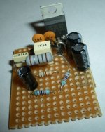
Here is a layout on stripboard I did for the 2030AV chip. It worked perfectly well but overall I had poor grounding (no real central point and small leads used) and managed to destroy this amp in a test using an earthed oscilloscope  . The layout is fine though if grounded properly and has been used at max volume for hours as an amplifier for en electric drum set. Note the ceramics right next to the chip and the 100uf caps on the side, these are essential!
. The layout is fine though if grounded properly and has been used at max volume for hours as an amplifier for en electric drum set. Note the ceramics right next to the chip and the 100uf caps on the side, these are essential!Attachments
Hi,
these chipamps all operate in ClassAB.
When there is zero input signal the output is just noise (mVac).
The quiescent current taken by the chip is given in the datasheet.
The transformer runs with just a tiny load and the smoothing caps have nearly peak voltage on them.
When a music signal is present the output might be around 1W. The PSU must supply that 1W of output + quiescent. The transformer still has a tiny load.
When the very rare occasions come along that require maximum power for a few fractions of a second the transformer does nothing extra. All the transient power comes out of the smoothing caps. The transformer then tries to charge the smoothing caps back up during each peak of the mains supply waveform. This recharging could coincide with with the max power peak or more likely the recharge will come soon after the peak power transient has passed.
The average load that the transformer sees is mostly the 1W+Quiescent. You will find that a PSU works well when the total maximum output power <=transformerVA/1.5, but, there is an acceptable economic range of VA.
I use VA between 1*total output power to 2* total output power. Most other builders work within this range.
I use VA between 1*total output power to 2* total output power
thanks for the explanation.
total output power means RMS, ok so I use 50VA (just!)?
So I am making it my final decision 180VA
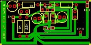
now the PCB #1, there may be some schematic mistakes. I'll correct 'em later. But friends, I'll request you to post your comments and suggestion regarding this PCB.
It was made using ExpressPCB. I think this is the best PCB designing software. In my xprience I found it more comfortable and easy to use software even than the well known Eagle
Attachments
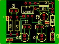
Suggestion: Move the LM1875 to the edge of the board so that a heatsink may be used.
Power supply scenerios:
With 144VA, it will handle Three LM1875 chips, IF there's -per each LM1875- 4700uF smoothing caps, per rail, at the power supply board. (and additinal 220uF or more per rail onboard the amp)
With 144VA, it will handle Two LM1875 chips, IF there's -per each LM1875- 2200uF (or more) smoothing caps, per rail, at the power supply board. (and additinal 220uF or more per rail onboard the amp)
With 72VA, it will handle Two LM1875 chips, IF there's -per each LM1875- 4700uF smoothing caps, per rail, at the power supply board. (and additinal 220uF or more per rail onboard the amp)
With 72VA, it will handle One LM1875 chips, IF there's -per each LM1875- 2200uF smoothing caps, per rail, at the power supply board. (and additinal 220uF or more per rail onboard the amp)
With 36VA, it will handle ONE LM1875 chip, IF there's -per each LM1875- 4700uF smoothing caps, per rail, at the power supply board. (and additinal 220uF or more per rail onboard the amp)
Production models quoted are at 28+28vdc, operating 4 ohm loads with audio at maximum. . . and generous heatsinks.
Efficiency for use of above figures depends on amplifier PCB--EDIT: So listen to Andrew on amplifier efficiency.
Accuracy for use of above figures depends on transformer quality (not a peak-rated or low-temp transformer).
Cheers!
Paswa said:So I am making it my final decision 180VA
now the PCB #1, there may be some schematic mistakes. I'll correct 'em later. But friends, I'll request you to post your comments and suggestion regarding this PCB.
It was made using ExpressPCB. I think this is the best PCB designing software. In my xprience I found it more comfortable and easy to use software even than the well known Eagle
hi Paswa.
The footprint of the LM1875 seems wrong to me. Are you intending to bend the leads to fit?
Increase the width of the traces, especially the ones that carry higher currents.
regards
danielwritesbac said:Production models quoted are at 28+28vdc, operating 4 ohm loads with audio at maximum. . . and generous heatsinks.
Hi Daniel,
Following up what Andrew said, read about regulation of toriods. Note how significant it is for small toriods (~20%). It will mean the output voltage of the PSU using the transformers you susgested will vary. I would also guess those small toriods will get quite warm.
regards
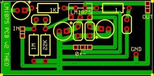
Where to begin?
Move and rotate C1 and C2 so that they connect as close as possible to the LM1875's power pins. Then bring a huge, fat ground trace (or a copper pour area) up to their ground ends. Also then rotate and move C3 and C4 up as far as you can, close to C1 and C2. It might help to move the power connector so it's aligned with the power pins.
Fatten all of your traces, by a LOT.
Add more connectors, so that the power supply decoupling ground, the output/zobel ground, and the signal ground, can each have their own completely-separate ground-return conductors, to the power supply. (Do some searches for 'star ground'.)
If you can squeeze R3 under the chip, that would probably be good. You can mount it on the bottom of the board.
Someone else will probably chime in, here, too. And there are already some threads with good discussions about PCB layout.
Greg Erskine said:
Hi Daniel,
Following up what Andrew said, read about regulation of toriods. Note how significant it is for small toriods (~20%). It will mean the output voltage of the PSU using the transformers you susgested will vary. I would also guess those small toriods will get quite warm. regards
Yes, that is a problem. Since production models were quoted, Toroid transformers aren't in use. A quality 105c rated, audio grade, EI core won't go above room temperature, in those scenerios, and attached to a chassis.
Toroid is quite different, with greater noise through the wire and also greater heat. So, do please increase the VA figure and also brace up the power supply filtering if using a toroid transformer.
gootee said:Someone else will probably chime in, here, too. And there are already some threads with good discussions about PCB layout.
Howabout this?
http://www.electronics123.com/s.nl/it.A/id.1801/.f
EDIT: R6 is erroneous value in that picture.
EDIT2: R4 and R5 are a "voicing" option that support component choices, and their values don't necessarily apply to your application.
EDIT3: FS1 and FS2 are erroneous because they couldn't be expected to operate simultaneously.
EDIT4: C1 pictured as circular, means electrolytic, and at that value its non-fidelity, so that should be either pictured as a square, or a larger value.
EDIT5:
and small EI transformers are even worse ~30%Greg Erskine said:read about regulation of toriods. Note how significant it is for small toriods (~20%).
Hi,
Your design is massively better than the first one. Positive and negative rails close together as you have them is very good. Seperate returns for the dirrerent ground currents is good. Decoupling caps close to the power pins is good.
However there are a few points that could still be improved.
It is good that you have seperated the current going to the smoothing caps and the current returned from the circuit at signal level, however it would be better if the return back to your power connector was taken from the center of the wire between the smoothing capacitors. This balances the rectified currents and helps to cancel out mains noise.
Also try to bring all of the other signals to one point (the star point) rather than spreading them out along the ground wire.
I have attached a rough modified version of your design (I used paint so please excuse the poor quality). Please note I have modified the Power connector so the ground is in the middle. If you can get the star point closer to the center of the two smoothing caps that would be better but paint didnt really make that very easy. Do not use the track between the smoothing caps as the star point it is better to have a small distance between the rectified current returns and the star point.
The +ve rail between the LM1875 pins looks like it will short out you may need to make this a bit thiner just in this area.
It looks to me like your input capacitor is too small but there is no value on it so I can't tell.
It would be worth getting your schematic reviewed before you go ahead with the PCB just in case there are any other problems.
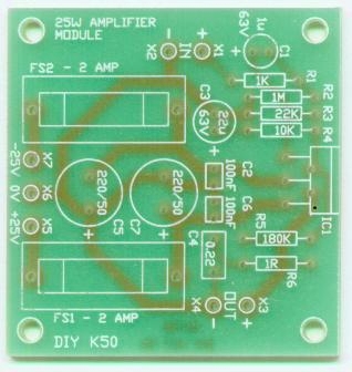
The DIY DK50 amp layout is OK but nothing special. It will work well but has not be optimised for the best sound quality. They have made the common mistake of beliving that the PSU GND pin is the star point when it should be the center of the two smoothing caps. Also returning the output ground to one of the capacitor pins means that the load return point has rectified currents flowing in it. I made this mistake on the first amplifer I made which worked fine but fixing it improved distortion by 6dB.
Regards,
Andrew
Your design is massively better than the first one. Positive and negative rails close together as you have them is very good. Seperate returns for the dirrerent ground currents is good. Decoupling caps close to the power pins is good.
However there are a few points that could still be improved.
It is good that you have seperated the current going to the smoothing caps and the current returned from the circuit at signal level, however it would be better if the return back to your power connector was taken from the center of the wire between the smoothing capacitors. This balances the rectified currents and helps to cancel out mains noise.
Also try to bring all of the other signals to one point (the star point) rather than spreading them out along the ground wire.
I have attached a rough modified version of your design (I used paint so please excuse the poor quality). Please note I have modified the Power connector so the ground is in the middle. If you can get the star point closer to the center of the two smoothing caps that would be better but paint didnt really make that very easy
. Do not use the track between the smoothing caps as the star point it is better to have a small distance between the rectified current returns and the star point.The +ve rail between the LM1875 pins looks like it will short out you may need to make this a bit thiner just in this area.
It looks to me like your input capacitor is too small but there is no value on it so I can't tell.
It would be worth getting your schematic reviewed before you go ahead with the PCB just in case there are any other problems.
The DIY DK50 amp layout is OK but nothing special. It will work well but has not be optimised for the best sound quality. They have made the common mistake of beliving that the PSU GND pin is the star point when it should be the center of the two smoothing caps. Also returning the output ground to one of the capacitor pins means that the load return point has rectified currents flowing in it. I made this mistake on the first amplifer I made which worked fine but fixing it improved distortion by 6dB.
Regards,
Andrew
Attachments
Hi,
the signal ground has it's own trace back to star ground.
The NFB route also has it's own trace to star ground.
Should the signal ground input pin go direct to the -ve pin of the DC blocking cap on the NFB route?
Should the trace from this DC blocking cap then have the option to add a low value resistor (or a wire link) between signal ground and star ground?
Hi,
The modifications look good. I see you have increased the size of the input cap to 2.2uF. However AndrewT is right some further improvement may be possible by keeping the input stage voltages closer together.
I have modified the drawing again to show this.
Th input filter signals are returned directly to the input ground and the input ground referance (NFB cap to ground) is tied directly to the input ground.
then there is a 0R link to the star ground. You may find 1 or 2 Ohms here works better but I have almost always found it better to not space the input and output off so I would start with 0R. If you get the grounding right in the first place there should be no need to space the input.
See rough drawing below.
Another point is you have no rectifier in this circuit, do you intend to rectify on a seperate PCB?
Regards,
Andrew
Attachments
Yes, no rectifiers. Those are only the local reservoir caps, for the amp's power pins. The main smoothing caps, and the entire power supply, are apparently on a different PCB. That is why I thought that all of the starred ground returns should leave this PCB separately, to go back to the star ground at the power supply before they meet. But it seems like it would be better to just put the power supply on the same PCB.
For example, look at posts #12 and #13, here:
http://www.diyaudio.com/forums/showthread.php?s=&postid=1387386#post1387386
Gfiandy and AndrewT (or anyone): If you have any opinions, comments, or suggestions for improving the layout at that link, I would appreciate your posting them, here (or there, if you prefer). (I thought that that layout was very, very nice. But I posted a few suggestions, in that short thread, mostly about the input section's loop areas. Comments or opinions on those suggestions would also be very welcome.)
- Status
- This old topic is closed. If you want to reopen this topic, contact a moderator using the "Report Post" button.
- Home
- Amplifiers
- Chip Amps
- LM 1875 questions