Hello, this is my first post here. First of al, sorry for my bad English.
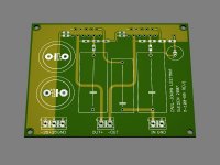
I’m now building my first serious amplifier, a bridged LM3886TF based on the schematic (BR100) of the Overture application note (1192) of National. Below are the schematics/boards that I draw. The power supply will be finished this week, and I just started drawling the amplifier board.
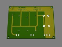
Here are the drawling of my power supply
I’m using a 500VA 22VAC Toroidal, and 50.000uF, witch will be enough.
And the amplifier
I have reed almost all topics in this sub forum according to the 3886, and they ware very useful. But my main question is, sins I don’t have any experience with the LM3886, is this schematic/board any good? Does anyone have any comments/improvements?
Greets
I’m now building my first serious amplifier, a bridged LM3886TF based on the schematic (BR100) of the Overture application note (1192) of National. Below are the schematics/boards that I draw. The power supply will be finished this week, and I just started drawling the amplifier board.
Here are the drawling of my power supply
An externally hosted image should be here but it was not working when we last tested it.
An externally hosted image should be here but it was not working when we last tested it.
I’m using a 500VA 22VAC Toroidal, and 50.000uF, witch will be enough.
And the amplifier
An externally hosted image should be here but it was not working when we last tested it.
An externally hosted image should be here but it was not working when we last tested it.
I have reed almost all topics in this sub forum according to the 3886, and they ware very useful. But my main question is, sins I don’t have any experience with the LM3886, is this schematic/board any good? Does anyone have any comments/improvements?
Greets
Two things immediately jumped out at me:
- The feedback loop (the trace running from the inverting input to the output, via Rf) is too long. This should be as short as possible. I would put Rf horizontal, immediately below the LM3886.
- A power trace is taking up space beyond the top of the LM3886. The board should end before here, otherwise you will run into trouble when you come to heat sinking it.
Other than this, the board doesn't look too bad.
Anton
Another couple of things:
- Cm is not in the signal path, so doesn't need to be a fancy film cap, a polar electrolytic will do just fine. Cm can also be shared between the two channels, and should be larger. Either 2x100uF, or one shared 220uF will do.
- Use a star ground. All the ground traces should lead to a single ground point. On your board, the ground trace for your supply decoupling capacitors goes to the LM3886 ground pin, then to ground. They should all go directly to ground. Research the term star ground on this site. Alternatively, use a ground plane.
Anton
Hi,
most of your diodes in the PSU are back to front.
Look at D5, 6, 7, 8, 9 and possibly D18.
The bridge rectifiers look OK.
T1 turns on RY2 after a delay. What is this doing?
Pin3 turns off RY1. What is this doing?
Where do out-2 & out-4 go to?
I don't like mains voltage going through a metal encased resistor. Are you happy with that?
+-30Vdc (it might be +-31Vdc) is right at the top end of powering 4r0 loads. Reactive speakers are an even worse load.
If you bridge with this supply voltage the combination will be right at the top end of current and voltage for driving an 8ohm speaker. The bridged amplifier may not like it.
amc184 said:Two things immediately jumped out at me:
- The feedback loop (the trace running from the inverting input to the output, via Rf) is too long. This should be as short as possible. I would put Rf horizontal, immediately below the LM3886.
- A power trace is taking up space beyond the top of the LM3886. The board should end before here, otherwise you will run into trouble when you come to heat sinking it.
Other than this, the board doesn't look too bad.
Anton
Thank you very much! This is information that really helps me.amc184 said:Another couple of things:
- Cm is not in the signal path, so doesn't need to be a fancy film cap, a polar electrolytic will do just fine. Cm can also be shared between the two channels, and should be larger. Either 2x100uF, or one shared 220uF will do.
- Use a star ground. All the ground traces should lead to a single ground point. On your board, the ground trace for your supply decoupling capacitors goes to the LM3886 ground pin, then to ground. They should all go directly to ground. Research the term star ground on this site. Alternatively, use a ground plane.
Anton
CJ900RR said:Looking pretty good. But use plains instead of traces for the power, one on each side. As in this design i did a while ago. I use smd-components and bigger caps but otherwise its much the same...
I’m sorry, but what are plains? My power traces are now 2,5mm / 0,1” width, isn’t that enough? To handle the current? I’ll be using circuit board with 35µm copper layer.CJ900RR said:And the other side...
You’re board looks very nice, have you got pictures of the finished amp?
Oops, the diodes are drawn wrong, you’re right. I’ll be edit the schematicAndrewT said:Hi,
most of your diodes in the PSU are back to front.
Look at D5, 6, 7, 8, 9 and possibly D18.
The bridge rectifiers look OK.
T1 turns on RY2 after a delay. What is this doing?
Pin3 turns off RY1. What is this doing?
The power_on (OUT-1) is to start the power supply. It turns RY2 (trough T1) and RY1 (trough IC3) imminently on. After a delay, RY1 will fall off. I already tested this cicuit, and it works just fine.
After I’m finished with this supply and amplifier board, I want to build a microcontroller (PIC12F675 or so) based “controller board”. With volume/tone control, display, maybe temps, and also controlling the power_on.AndrewT said:Where do out-2 & out-4 go to?
I don’t see the problem in that?AndrewT said:I don't like mains voltage going through a metal encased resistor. Are you happy with that?
I know, I design this amp for 8ohm speakers. Ideal would be 28VDC, but I got good heat sinking, and I lose some more voltage over my rectifiers at high currents. So I think that wouldn’t be a problem.AndrewT said:+-30Vdc (it might be +-31Vdc) is right at the top end of powering 4r0 loads. Reactive speakers are an even worse load.
If you bridge with this supply voltage the combination will be right at the top end of current and voltage for driving an 8ohm speaker. The bridged amplifier may not like it.
At 0.1 amps
22 * √2 - 0.6 = 30.5V
At 8 amps (4 per amplifier)
22 * √2 – 1.4 = 29.7V
An externally hosted image should be here but it was not working when we last tested it.
Thanks!sukyone said:good looking
I started building my “capacitor rack”, it’s a little bit different than I draw, but it quite matches.
An externally hosted image should be here but it was not working when we last tested it.
robertj88 said:I started building my “capacitor rack”, it’s a little bit different than I draw, but it quite matches.
An externally hosted image should be here but it was not working when we last tested it.
Insulate the exposed metal can of the caps from the metal "seat" they are resting on. The can usually leaks towards the negative potential.
The metal encased mains carrying/passing resistor is attached to what?
your 22Vac transformer will have a much higher output voltage at quiescent current than you've shown.I know, I design this amp for 8ohm speakers. Ideal would be 28VDC, but I got good heat sinking, and I lose some more voltage over my rectifiers at high currents. So I think that wouldn’t be a problem.
At 0.1 amps
22 * √2 - 0.6 = 30.5V
At 8 amps (4 per amplifier)
22 * √2 – 1.4 = 29.7V
The sag in voltage at maximum output will be much higher than you've allowed for.
That schematic is a recipe for disaster.I would'nt recommend using it unless you want to see how some caps and chips fry just for show.Hello, this is my first post here. First of al, sorry for my bad English.
I’m now building my first serious amplifier, a bridged LM3886TF based on the schematic (BR100) of the Overture application note (1192) of National. Below are the schematics/boards that I draw. The power supply will be finished this week, and I just started drawling the amplifier board.
Here are the drawling of my power supply
An externally hosted image should be here but it was not working when we last tested it.
An externally hosted image should be here but it was not working when we last tested it.
I’m using a 500VA 22VAC Toroidal, and 50.000uF, witch will be enough.
And the amplifier
An externally hosted image should be here but it was not working when we last tested it.
An externally hosted image should be here but it was not working when we last tested it.
I have reed almost all topics in this sub forum according to the 3886, and they ware very useful. But my main question is, sins I don’t have any experience with the LM3886, is this schematic/board any good? Does anyone have any comments/improvements?
Greets
That schematic is a recipe for disaster.I would'nt recommend using it unless you want to see how some caps and chips fry just for show.
Perhaps a bit more specific comments would be more helpful? Like, what problems do you see, and how would you fix them?
I would suggest building two boards one lm3886 on both . It will be easier for you to get a good layout it is good to keep + _ power traces together. keep fb loop very very short even solder fb resistor direct to the ic. keep inputs and outputs as far away from each other as possible. also keep input away from power traces. pin 7 should go to power ground also the ground side of the 0.1uf decoupling capacitors direct to power ground.
I am a newbie but i hope this imformation is of use to you .
Good luck Ian
I am a newbie but i hope this imformation is of use to you .
Good luck Ian
no need to excuse your self as a Newbie.I would suggest building two boards one lm3886 on both . It will be easier for you to get a good layout it is good to keep + _ power traces together. keep fb loop very very short even solder fb resistor direct to the ic. keep inputs and outputs as far away from each other as possible. also keep input away from power traces. pin 7 should go to power ground also the ground side of the 0.1uf decoupling capacitors direct to power ground.
I am a newbie but i hope this imformation is of use to you .
Good luck Ian
All of your advice comes from reading good resources. Keep informing yourself and you'll soon be experienced. You have already passed Newbie status.
- Status
- This old topic is closed. If you want to reopen this topic, contact a moderator using the "Report Post" button.
- Home
- Amplifiers
- Chip Amps
- My Bridged LM3886