

Hi boob_v5,
well the amp can deliver only 20W@8Ohm, therefore quite sensitive speakers are recommended. The main feature of this construction is a speed and high resolution exceptional in mid and treble ranges.
Assembly point of view one bottleneck has to be mentioned, reflow oven is needed because of soldering of power/thermal pads.
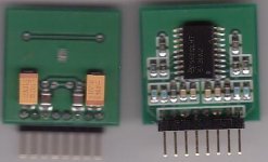
Attachments
20w would be plenty as I'm using old speakers that were not designed for much power anyway. I think you may have misunderstood one of my questions, I was hoping you could provide me with a copy of the file you used to etch the pcb's, ie the picture of the actual tracks on the board. As for the reflow oven I know that there is one in my university, will have to try and bribe my teacher into letting me use it.....
It's not that hard to solder by hand.mzperx said:Assembly point of view one bottleneck has to be mentioned, reflow oven is needed because of soldering of power/thermal pads.
http://sjostromaudio.com/hifi_pics/hifi_100pr/qrv07r0_TPA6120.jpg
http://sjostromaudio.com/hifi_pics/hifi_100pr/qrv07r0_TPA6120_backside.jpg
I write this:
This part needs to be soldered into the large pad on the pcb. To do this you must use lot's of heat. If you have two soldering irons, use both at the same time. The buffer gets it's cooling via this pad so it's important that the buffer is very good soldered. When I soldered this IC, it turned out not to be so difficult. Solder the pins as usual. Then solder the backside. Turn up the soldering iron to max temperature, like 450 deg C in my case. Warm and add tin and continue to warm for 10-20 seconds or so. Notice how the tin gets sucked up through the via holes. You can "burn" quite a lot and the upper side won't melt.
At my 1st version I have tried to solder manually a power pads, but after X-ray controll I have to say that this methode gives absolutely non adequate solder joint. In best case the tin could touch the power pad more or less, but never could solder the acceptable min 50-75% part of surface of the related pad.
However if one huge via (with2-3mm inner diamater) is applied in center of power pad instead of by application note recommended more and smaller vias, than it can be already manual solder friendly solution.
However if one huge via (with2-3mm inner diamater) is applied in center of power pad instead of by application note recommended more and smaller vias, than it can be already manual solder friendly solution.
nelsonvandal said:Has anybody tackled the DC-offset issue yet? I'm about to build a TPA6120 amp for headphone use.
Without resorting to additional DC servo circuitry the best you could do
is keep the feed back resistors as low as possible, this will however result in a rather low input impedance if your source/ preamp could handle this no problem.
You will find that the DC offset is proportional to the value of the above mentioned resistors so lets hope you are not using Grado headphones
in which case 10mV might already be a problem. In short its a compromise between what you could accept as a reasonable input impedance and the DC offset that you are prepared to live with.
Old thread I realize, but interesting to find it.
Have a 4-out headphone amp in the mail, with each of the channels using the TPA6120 I thought to have understood. With some summing-wiring (and all controls set identical) could then function as a mini-speaker amp as well, nice.
Rout of those is 10 Ohms each, so that'll give some less power than your 2 Ohm summing version.
and now the schematic package is attached as well.
Meantime some significant improvements were performed:
The amp has got a new fully symetrical input stage (w OPA1632) and the output resistors were decreased from 10R to 2R. So the total outout resistance is already only 0.1 Ohm.
Have a 4-out headphone amp in the mail, with each of the channels using the TPA6120 I thought to have understood. With some summing-wiring (and all controls set identical) could then function as a mini-speaker amp as well, nice.
Rout of those is 10 Ohms each, so that'll give some less power than your 2 Ohm summing version.
- Status
- This old topic is closed. If you want to reopen this topic, contact a moderator using the "Report Post" button.
- Home
- Amplifiers
- Chip Amps
- parallel TPA6120?