Well I just finished my first PCB design of a small 1W stereo amplifier. I really didnt have much of an idea of what I was doing, and it would be stupid to order boards that didnt work, so I was wondering if anyone could inform me of any errors, (Im sure there will be plenty) or tips to make my board better. The original schematic is on this page. My PCB picture will be attached. Please take a look. Thanks.
Attachments
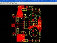
Actually, the input signal ground and the chip's ground need to be connected to all the other grounds too.
Other suggestions would include using thicker traces, using 45 degree bends instead of 90 degree bends, and tidying up the traces. It looks like you've made a double sided board but you can do this using a single sided board if it will cost less.
Other suggestions would include using thicker traces, using 45 degree bends instead of 90 degree bends, and tidying up the traces. It looks like you've made a double sided board but you can do this using a single sided board if it will cost less.
A double sided board is a board with copper on both sides. Traces run on both layers and parts may be on one or both sides of the board.
Thicker traces have lower resistance and can carry higher current. For your specific application thick traces are not needed but it would not hurt to make them thicker.
45 degree bends in traces have a better chance of being etched properly than 90 degree bends do. Board houses have improved in this area but it is still generally better to use bends that are 45 degrees or less where possible, especially if you plan on etching your own boards.
- Status
- This old topic is closed. If you want to reopen this topic, contact a moderator using the "Report Post" button.