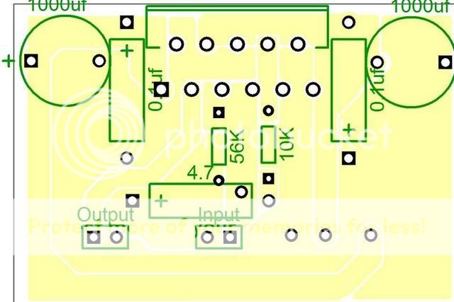
This is the PCB, the power supply pins did not label this morning... But from left to right they are
0v -24v +24v
The Schematic
I have built this according to the schematic on the Decibel Dungeon site and is one sided for conveniance. I aim to etch this myself, though will develop it into a more complete board, with preamp etc on the same board.
The filter to safety ground is missing, as I will have 1 filter for all the amp stages.
The connection from Signal Gnd to Power Gnd (0v) is currently missing from the PCB also. I'm looking for advice on how I should execute this. My own thought is a .25mm trace from square pad on the input pins to the 0v line adjacent. Is this fair enough?
By the way the caps are orientated the way they are to allow me to mount them on their sides. I want to make the board profile as flat as possible as this will be part of a 160mm by 100mm board that fits in a hammond extruded alu case.
Comments please?
BWRX said:Hi blair. After a quick glance it appears that there is no feedback resistor connected to the output. It's hard to tell with that peach color, but are the input signal and power supply grounds connected?
Ye sorry, I should have mentioned in the preamble that the feedback resistor is going straight onto the LM3875 pins...
The input signal and power supply grounds are yet to be tied together. I was referring to that in my question above, what is the best way to tie these, I had thought a very thin (.25mm) trace between the input and power supply ground?
Other than that anything obvious that can be improved?
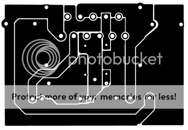
Here is a high contrast version of the bottom of the board...
Some things I did for my layout with the LM3875:
Locate both supply caps to the left of the chip. Remove pin 2 (and the through hole on the board) so you can run a thicker power trace to pin 4. Use supply rail decoupling caps with a smaller package. Mount the feedback resistor on the board instead of directly to the pins of the chip. There should be ample room for this. Connect the power and signal ground using a plane, just keep the signal ground away from the high current paths around the supply caps and output speaker ground. This shouldn't be hard to do if you locate the power ground on the left side of the board between the caps and have the signal ground on the right side of the board. I may have time tomorrow to whip up a quick layout if that didn't make sense.
Locate both supply caps to the left of the chip. Remove pin 2 (and the through hole on the board) so you can run a thicker power trace to pin 4. Use supply rail decoupling caps with a smaller package. Mount the feedback resistor on the board instead of directly to the pins of the chip. There should be ample room for this. Connect the power and signal ground using a plane, just keep the signal ground away from the high current paths around the supply caps and output speaker ground. This shouldn't be hard to do if you locate the power ground on the left side of the board between the caps and have the signal ground on the right side of the board. I may have time tomorrow to whip up a quick layout if that didn't make sense.
BWRX said:Some things I did for my layout with the LM3875:
Locate both supply caps to the left of the chip. Remove pin 2 (and the through hole on the board) so you can run a thicker power trace to pin 4. Use supply rail decoupling caps with a smaller package. Mount the feedback resistor on the board instead of directly to the pins of the chip. There should be ample room for this. Connect the power and signal ground using a plane, just keep the signal ground away from the high current paths around the supply caps and output speaker ground. This shouldn't be hard to do if you locate the power ground on the left side of the board between the caps and have the signal ground on the right side of the board. I may have time tomorrow to whip up a quick layout if that didn't make sense.
Thanks for that. Unfortunately
") its GF night tonight, so I wont get a chance to try some of those ideas till tomorrow...
its GF night tonight, so I wont get a chance to try some of those ideas till tomorrow...theAnonymous1 said:What software did you use to make the layout?
I used Diptrace, so far my favourite designer. I found it a lot easier than Eagle and a fair bit better than PCB123. This is my first audio PCB, previously I have made sensors etc, marks out of 10?
Thanks for the comments so far any other ideas are welcome as well..
Here is my second attempt
After pondering some of BWRX's advice, I came up with a second design.
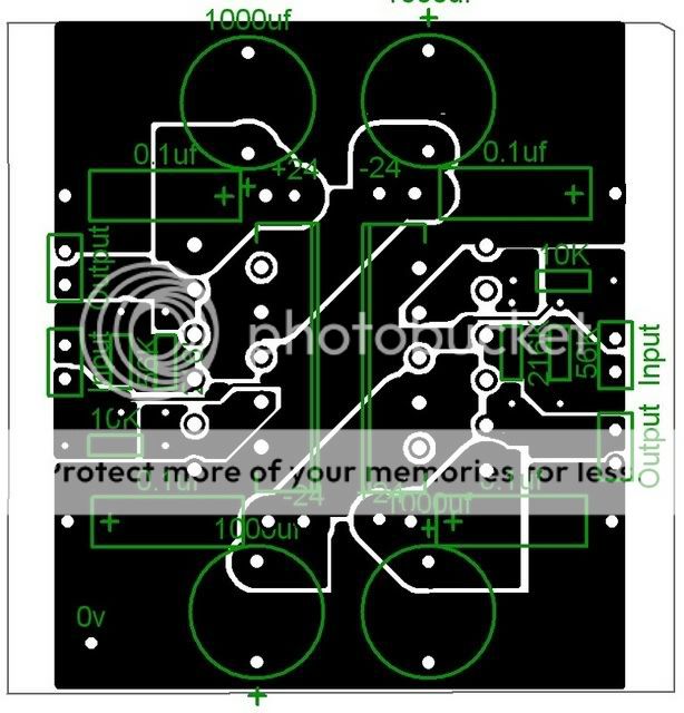
The design is for a pair of chips. This time the power rails are thicker, and the decouling caps on the left of each chip. I have mounted the resitor on the board.
I have omited the input caps. I will filter dc out (if necessary) further up the signal chain.
The signal ground and power gound are now connected,
This is designed for use with a single power supply.
I have connected several of the NC pins to the power ground to make the routing easier.
The two chips will share a heatsink, which I will also couple to the alu case I have in mind....
Comments please, before I start the next section of my design...
After pondering some of BWRX's advice, I came up with a second design.
The design is for a pair of chips. This time the power rails are thicker, and the decouling caps on the left of each chip. I have mounted the resitor on the board.
I have omited the input caps. I will filter dc out (if necessary) further up the signal chain.
The signal ground and power gound are now connected,
This is designed for use with a single power supply.
I have connected several of the NC pins to the power ground to make the routing easier.
The two chips will share a heatsink, which I will also couple to the alu case I have in mind....
Comments please, before I start the next section of my design...
Have you researched the actual sizes and lead-spacings of all of the components? What make/model/voltage caps are you using for the 1000uF positions? And what type are the 0.1uF polypropylenes?
- Tom Gootee
http://www.fullnet.com/~tomg/index.html
- Tom Gootee
http://www.fullnet.com/~tomg/index.html
gootee said:Have you researched the actual sizes and lead-spacings of all of the components? What make/model/voltage caps are you using for the 1000uF positions? And what type are the 0.1uF polypropylenes?
- Tom Gootee
http://www.fullnet.com/~tomg/index.html
The lead spacings are pretty general just now, which I think is fine for the resistors, but as you have pointed out the big electolytics are on the small side.
The design is such though that I can accomodate larger, or even multiple electrolytics with 5-10 minutes of alterations to the board.
Consider this a rough sketch. I am going to add buffers etc over the next few days. My aim is to work in a modular fashion so that I can easily produce a range of pcbs for trying out.
Right nowI am intersted in any electrical/layout mistakes such as grounding, trace widths etc
woolly said:amateur opinion - would be better with more space between tracks or could be a tricky when soldering and spilling over tracks
I use liquid flux/cleaner when soldering onto pcb. I never have any issues with spill over.
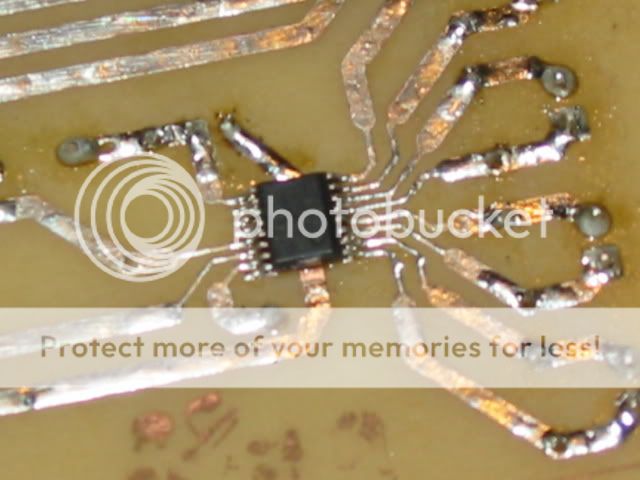
Here is a chip that I soldered (prior to clean up). Its 5mm long and has 16 pins. If you use flux, the solder looks after itself... No bridges. I am very amateur, if I can do it anyones pet monkey could have a go!
The reason why I have gone for such small gaps (4mm) is that it saves time and solution when it comes to etching. I plan to do the etching at home...
justblair said:
The lead spacings are pretty general just now, which I think is fine for the resistors, but as you have pointed out the big electolytics are on the small side.
The design is such though that I can accomodate larger, or even multiple electrolytics with 5-10 minutes of alterations to the board.
Consider this a rough sketch. I am going to add buffers etc over the next few days. My aim is to work in a modular fashion so that I can easily produce a range of pcbs for trying out.
Right nowI am intersted in any electrical/layout mistakes such as grounding, trace widths etc
OK. I understand.
I have not checked the actual connections. But, overall, I like your layout philosophy, in the last one you showed.
When you get to the point of selecting components, you might want to consider the (nice and small) WIMA MKP2 (IIRC) polypropylenes, which have LS of only 5mm and length of only 7mm. The 0.22uF ones are only 7mm x 7mm, for example. Mouser.com has them for pretty cheap prices.
A couple of other concerns:
1. I am not sure that you will want your power and signal grounds connected as you have them. Unless I'm missing something, I think I would prefer that they make their ways separately back to the power supply's cap gnd, or the star ground which will probably be in that vicinity.
I could easily be wrong about that. BUT, you could fairly-easily just CHECK which way is better, with LT-Spice (for example), by modeling each of the traces and wires as a resistor and inductor in series, using ballpark figures of 25nH and .001 Ohms per inch, at least at first. There's no good LM3875 spice model, that I know of. But you can use TI's OPA541E model as a pretty good approximation, for these types of purposes.
See http://www.fullnet.com/~tomg/gooteesp.htm , for ready-made downloadable LT-Spice files with basically everything you need to get you started immediately.
You could even have Spice compare the output distortion (e.g. THD @ 20 kHz) for different wiring and grounding schemes, as well as just eyeball the currents and the induced noise/ripple/voltages, etc, when various grounds share conductors that have their impedances modeled.
You can also model the power supply lines' impedances. It's very useful, and interesting, to be able to compare different capacitors, e.g. with better or worse ESR, and to compare results for different values of bypass caps, and results with and without snubbers, etc etc etc.
It shouldn't be too much work, even if you've never used Spice. And if you need any help with it, I'll be glad to try to be of more assistance. (And note that LT-Spice schematics are easy to bat back and forth, because they are just text files.)
Simulating with the ground-return conductors' impedances can certainly enable one to be more comfortable with a design, by helping them to be more sure that they haven't inadvertently let the wrong currents share a ground return, which can have surprisingly-large effects.
Modeling your conductors' impedances is also great for identifying any traces or wires where length/size/i.e.impedance are more critical than most, which can help you to create the best-possible PCB layout.
LTspice can even use WAV files for the input (and output) signals! So, using your computer's sound card, you could even do some sort of listening comparisons of the actual SOUNDS of different wiring configurations, and component choices, etc (keeping in mind that the modeling isn't perfect, of course; But it might be useful for relative comparisons.).
Sorry to have blathered-on for so long, about all of that.
2. Are you sure that there is enough space for a big-enough heatsink, between the chips? That might be an area where you'll need to get exact measurements, etc, and adjust your PCB a little, later on.
3. Also, if you can, you might want to slide your inputs and outputs a little farther apart, or even consider taking your outputs straight up and out, from closer to the pins. It looks like the inputs could at least be moved away from the outputs, a little, and the output traces fattened, more. Actually, I'd try to keep everything else away from the output traces, too, as much as possible. Power IN traces could easily be pulled away from the output traces, a little more, for example.
4. You could clip off pins 9, 10, 11, too, and have better input and ground traces. Pins 2, 5, and 6 could go, too.
- Tom Gootee
http://www.fullnet.com/~tomg/index.html
Thanks Tom for taking an interest. As you may have guessed I am new to PCB design, though eager to learn. My previous designs have been simple measuring circuits (above was a temperature measuring circuit) and simple voltage regs.
In response to your comments
1. I take that on board. I will run the signal ground traces back further. My idea was that the middle of the pcb was sort of a star ground point. But I get confused (as do all noobs it seems) with grounding arrangements...
2. Heatsink wise, i measured up around a heatsink salvaged from a power supply. It is sort of a T shape, with additional horizontal strokes
T
T
I
If you get my drift. It is pretty unsubstantial, though my thought was to couple the horizontal top with the Alu box's casing to make it a bit better. I will keep my eye out for something more substantial, as you say, (and I had already had in mind when I designed) I can widen the design further if a better source is found.
3. I see what you mean, and I think you are right. I am building an evolution of the design using Pedja rogics jfet buffer. I will see what I can do with this.
4. i had considered clipping the pins, the reason I chose to connect them to ground instead was that I aim to use a bit of pressure (by stressing the board ever so slightly to push the heatsinks onto the top of the case. I have not experimented with this yet. Leaving the pins on I thought would lead to more even pressure on the heatsink/case. It might be better though with pins snipped. Then the pins of the chip might flex as well. The pressure i refer to is very small. I will use some grease to couple as well.
As for using LTspice.
I saw that diptrace supports simulation with Spice. I know that i should start learning it, my ambitions are some time (In the long term future) to become semi pro in my abilities. But I am at the bottom of the pole right now. I will perhaps give it a go, though i may need some hand holding!
I have also considered going to double sided board design....
My rig for developing PCB's is crude (but effective)

Its a 650w OHP with an exposure time of 8 1/2min. Which gives reasonable detail (down to .5mm traces so far)
I have not tried double sided, but it would open up more opportunities for mistakes.. I mean design improvements.
I am thinking i can get the whole amp in a 100mm*160mm*55mm case if I use a moderate rated transformer. I had planned on a seperate case for the tranny, but if i can squeeze it smaller, My Gf will be pleased.
In response to your comments
1. I take that on board. I will run the signal ground traces back further. My idea was that the middle of the pcb was sort of a star ground point. But I get confused (as do all noobs it seems) with grounding arrangements...
2. Heatsink wise, i measured up around a heatsink salvaged from a power supply. It is sort of a T shape, with additional horizontal strokes
T
T
I
If you get my drift. It is pretty unsubstantial, though my thought was to couple the horizontal top with the Alu box's casing to make it a bit better. I will keep my eye out for something more substantial, as you say, (and I had already had in mind when I designed) I can widen the design further if a better source is found.
3. I see what you mean, and I think you are right. I am building an evolution of the design using Pedja rogics jfet buffer. I will see what I can do with this.
4. i had considered clipping the pins, the reason I chose to connect them to ground instead was that I aim to use a bit of pressure (by stressing the board ever so slightly to push the heatsinks onto the top of the case. I have not experimented with this yet. Leaving the pins on I thought would lead to more even pressure on the heatsink/case. It might be better though with pins snipped. Then the pins of the chip might flex as well. The pressure i refer to is very small. I will use some grease to couple as well.
As for using LTspice.
I saw that diptrace supports simulation with Spice. I know that i should start learning it, my ambitions are some time (In the long term future) to become semi pro in my abilities. But I am at the bottom of the pole right now. I will perhaps give it a go, though i may need some hand holding!
I have also considered going to double sided board design....
My rig for developing PCB's is crude (but effective)
Its a 650w OHP with an exposure time of 8 1/2min. Which gives reasonable detail (down to .5mm traces so far)
I have not tried double sided, but it would open up more opportunities for mistakes.. I mean design improvements.
I am thinking i can get the whole amp in a 100mm*160mm*55mm case if I use a moderate rated transformer. I had planned on a seperate case for the tranny, but if i can squeeze it smaller, My Gf will be pleased.
Hi blair.
Now that you changed the layout to two chips on one board it would be advantageous to give each chip it's own separate ground plane. I know symmetry is very appealing but it doesn't always produce the best layout. You want the signal and power grounds connected but only at one point, preferably near the speaker ground. You want the grounds of the large electrolytic caps, the smaller film bypass caps, and the speaker ground close to each other. You also want the film bypass caps as close to the chip's power pins as possible. These requirements conflict with each other a bit, and making good compromises is what a good layout is all about.
Also as Tom mentioned, and I have said this before too, why not remove pin 2 so you have better access to pin 4? Removing pin 9 would also free up access to pin 8. I'd keep the rest though for mounting stability.
BWRX said:Hi blair.
Now that you changed the layout to two chips on one board it would be advantageous to give each chip it's own separate ground plane. I know symmetry is very appealing but it doesn't always produce the best layout. You want the signal and power grounds connected but only at one point, preferably near the speaker ground. You want the grounds of the large electrolytic caps, the smaller film bypass caps, and the speaker ground close to each other. You also want the film bypass caps as close to the chip's power pins as possible. These requirements conflict with each other a bit, and making good compromises is what a good layout is all about.
Also as Tom mentioned, and I have said this before too, why not remove pin 2 so you have better access to pin 4?
Thats no problem to do. I figured that because they shared the same power source there would be no difference if they shared the same ground.... But clearly I have a bit still to learn... The grounding just melts my head!!!?

I'm going to spend a bit of time thinking this through, taking what you have said on board and chosing some components. I have put together the bulk of a (Pedja Rogic) schematic which adds a jfet buffer to the circuit. I think also working in two planes will solve some issues (and create some more no doubt)
But I am glad to have you both on board with some advice. Learning this stuff is slow going for me, its nice to have someone there to point me in the right direction. Thanks chaps.
Regards
Blair
ps. That pin will probably disapear in the next incarnation. Though one question.. Does connecting a power or gorund pin to a NC pin cause any issues? I have sort of an idea in my head here....
justblair said:I figured that because they shared the same power source there would be no difference if they shared the same ground.... But clearly I have a bit still to learn... The grounding just melts my head!!!?
There shouldn't be a problem with two chips sharing the same ground and the same power source. Most people have a system that is like this. The key is to avoid forming ground loops. That's where the whole star grounding concept comes into play.
justblair said:Does connecting a power or gorund pin to a NC pin cause any issues? I have sort of an idea in my head here....
That shouldn't be a problem but still I wouldn't do it. It's easier just to remove the pin if it's in the way.
- Status
- This old topic is closed. If you want to reopen this topic, contact a moderator using the "Report Post" button.
- Home
- Amplifiers
- Chip Amps
- Single Sided LM3875 PCB... Crit please.