I had a lady bring me one of these amps desperate to get sound back in her Lexus. Figured I'd at least give it a look see. Haven't done anything yet except a visual inspection. Only thing I see is a very, and I mean very, small SMD capacitor missing from near one of the ground pads through which a screw mounts the board to the chassis. I'd guess that this shunts some high freq noise to ground and isn't likely the cause of a non functional amp. I would have thought it just a burned trace but a couple of the other pads still have their capacitor and I realized this pad is missing one.
The normal searches don't turn up any helpful info but it does turn up a lot of ads offering repair of these amps, so I'm figuring that there is money to be made on this amp. Any body know anything about this amp that could help out or save me some grief before I power it up and dive in?
The normal searches don't turn up any helpful info but it does turn up a lot of ads offering repair of these amps, so I'm figuring that there is money to be made on this amp. Any body know anything about this amp that could help out or save me some grief before I power it up and dive in?
Well I went ahead and put power to it. I've got +32V and -32V but the protection shuts it down in about 3-4 seconds. I can watch pin 2 of the 2525 chip go from 5V to 1.6 so it looks like the protection doesn't like something. I'm going to re-read the protection circuit troubleshooting to get some ideas but am still open to advice.
Don't know if its normal or not but the negative rail caps bleed down pretty quick but the positive seem to hold voltage a lot longer after shutdown.
Don't know if its normal or not but the negative rail caps bleed down pretty quick but the positive seem to hold voltage a lot longer after shutdown.
It's hard to get into repairing OEM equipment because the manufacturers use components with their own markings and won't supply parts or service literature. Add to that that some require digital communications (copper or fiber interface) with other components.
Look for shorted output transistors or DC offset on one channel.
Look for shorted output transistors or DC offset on one channel.
Checking for DC offset was a good tip. One of the channels, (there is 8 of them) goes to about -14V before the protection shuts it down. Figured the first step would be to pull the output transistor. Well that didn't do it. There is still negative voltage leaking through to the speaker output. There is a TO-92L transistor that drives the gate of the output transistor and it is also being driven way negative even with the output transistor out of the circuit. There is an electrolytic cap and a couple other TO-92 transistors related to the circuit, otherwise its mostly very small SMD components. I'm suspicious of the electrolytic but of course very open to suggestions.
The up side I guess is that there are 8 channels pretty closely mirrored nearby to make comparisons from.
The up side I guess is that there are 8 channels pretty closely mirrored nearby to make comparisons from.
Managed to spend a little more time on the amp before it got cold enough to call it a night. A couple of observations.
With the PNP output transistor out of the circuit, the negative voltage ~-14V stayed on the output. With the TO-92L (a 1W PNP) that is connected to its base out of the circuit, the speaker output goes to full positive voltage ~+32V. It tested ok out of the circuit so I put it back in and pulled the NPN output. With both output transistors out of the circuit (only 1 NPN and 1 PNP per channel) the DC on the speaker output goes to ~-4V which doesn't trigger protection.
At this point with the amp out of protection and able to be powered for more than a few seconds at a time, I'm planning to pull the outputs from the adjacent working channel. From there I'll start pulling and or swapping components working backwards from the outputs. Hoping against hope that I find something in the thru hole parts. Most of the SMD stuff on this board is absolutely microscopic.
Man this thing is kicking my butt. I have 8 independent channels that are pretty much the same and one has a pervasive negative voltage throughout.
With the output transistors removed the PNP output has neg rail -32v on the collector and the NPN has positive rail +32v on its collector. This is good.
Both bases have -31v, both emitters have -4.4V This is bad.
The PNP's base driver has neg rail on all pins (swapping with good channel doesn't change)
The NPN's base driver has neg rail on base and emitter with pos rail on the collector
In the good channel the base and emitter of these drivers are very low voltages ~1v, -1v
Two other transistors are nearby, function undetermined.
The one on the PNP side has neg rail on all pins, the NPN side has neg rail on collector with pos rail on emitter and base.
There is an SMD transistor between the outputs, suspect it is for bias. Neg rail on all pins. On good channel no neg rail on any pin.
Small electrolytic cap in the middle, neg rail on both sides
If this adds up to anybody, I'd appreciate any help. I realize what a long shot this is.
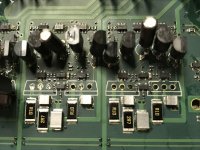
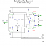
The first discrepancy is that there are no resistors between the base drivers and the output transistors. The second is that I don't seem to have +-15 anywhere, instead +- 34-35 V that isn't from the rail supply which is ~+-32V. I haven't traced the circuit much beyond the drivers as the mix of thru hole and SMD has me super dreading that task but drawing out the circuit is pretty high up on the to do list at this point. I'm nervous that this my be a multi layer board also. I haven't seen any mid layer traces where light goes through the board but a few traces do seem to dead end, though it may just be that my brain is getting fried staring into the abyss of this board.
The only thing I'm certain about is the outputs and the drivers. I get lost trying to trace further without drawing it out. There is only 2 other through hole transistors which I'd assume are the equivalent to the pre-drivers in the schematic. The SMD between the outputs I ASSume is for bias. There are a couple SMD 3 pin devices but the id comes back as double diode rectifiers. I'd be suspect of that id but the numbers even show opposite polarity between + and - sides of the circuit. There is also a double diode of mixed polarity which is the one connected near the output and I'm suspecting it as part of the feedback. I still could be totally off on the double diode id though.
- Home
- General Interest
- Car Audio
- Lexus Factory amp Mark Levinson