email sent.
I accidentally destroyed one of the a1275's removing it for testing, but thats alright because I'm pretty sure it was bad after testing the other (is there a common set of transistors that I can replace these with or is it time to put them on the Parts order list?)
undamaged a1275
red lead on base black lead on collector I get 1.001v
red lead on base black lead on emitter I get OL
q7
red lead on base black lead on collector I get 0.6v
red lead on base black lead on emitter I get 0.6v
and OL on every other combination
q7a was just a repeat of all of the q7 readings
red lead on base black lead on collector I get 0.6v
red lead on base black lead on emitter I get 0.6v
and OL on every other combination
the FETs are blown too, I cut em out and tested a few, they all tested bad... again
I will go ahead and find and order bd139s, bd140s, and another set of irf3205s
looks like I'm on hold till further notice when parts arrive, probably after thanksgiving sometime.
I have lots of pieces parts on hand, but not a single spare replacement to anything I've pulled from this amp so far.
I will go ahead and find and order bd139s, bd140s, and another set of irf3205s
looks like I'm on hold till further notice when parts arrive, probably after thanksgiving sometime.
I have lots of pieces parts on hand, but not a single spare replacement to anything I've pulled from this amp so far.
Thank you for the email Perry. I appreciate it. after looking over the schematic and my board I can see how these amps are quite alike. The power section is nearly identical, down to the component designations and type.
Is there anything else I can check right now with the board disassembled the way that it is?
I believe I found the bd139s and bd140s semi locally (more local to work) and will pick them up tomorrow evening perhaps. but I will have to wait on another order of the irf3205s
Is there anything else I can check right now with the board disassembled the way that it is?
I believe I found the bd139s and bd140s semi locally (more local to work) and will pick them up tomorrow evening perhaps. but I will have to wait on another order of the irf3205s
I got the bd139s and bd140s, but I noticed that they were only rated at half of the power of the original a1275 and c3228s, so I also picked up another different set of mje340s and mje350s rated at almost twice the original power of the a1275s and c3228s (could not find the originals for the life of me tho)
which would be the better choice as replacements? the BDs or the MJEs?
the irf3205s will be here friday
which would be the better choice as replacements? the BDs or the MJEs?
the irf3205s will be here friday
BD's it is then. I spent a good deal of time tonight de-soldering the board for all these fancy new parts... I've never cleaned anything electronic up as good as I did this board.
I will get the drivers in tomorrow after work and check to see if I have a good signal on the gate pads.
Good signal should be something like a 22.5kHz square wave right?
and bad signal would be no signal or just high or low voltage, probably very near 12v right?
I will get the drivers in tomorrow after work and check to see if I have a good signal on the gate pads.
Good signal should be something like a 22.5kHz square wave right?
and bad signal would be no signal or just high or low voltage, probably very near 12v right?
Alright, I got the irf3205s in the mail today, 2 days early. I placed the bds in and soldered them in, put the board back in the heat sink and clamped the remainder of the FETs down, used a regular automotive 10 amp fuse in line with the B+ wire, and wired it to a big dry cell battery.
when powered with remote I still get a quick flash of the protect LED and a few seconds later the internal relay clicks on. Just like before.
I used my scope on the gate pads for the FETs and I see a decent looking signal (scope does not have great resolution at all) but as far as I can tell it might only be 180-210Hz according to the scope, but it says 25kHz flat with my DMM... (I think I'll only trust the waveform on my scope)
Shall I install the FETs now? I'm also guessing that the circuit doesn't completely power until the missing FETs turn on and supply power elsewhere to the circuit, and that's why I'm only seeing the boot procedure I'm seeing without a power LED lit?
The power led doesn't have power until the one transformer is getting power from the 3205's. (the one closest to the speaker leads in your pictures). I wouldn't worry about this until you have some of the 3205's populated. If your gate signals coming from your new bd139/140 pairs looks good, you can get away with putting only two 3205's in on that left transformer as a test. Put the middle two in as this will probably get you one on each side of the gate drive signal. This way when you power it up and *if* something else is shorted you don't risk wiping out so many 3205's in the process, only 2.


The 1k resistors would be used to load the drive signal to confirm that it's as it should be. With no FETs in the circuit, it's not always possible to see if there is a problem.
Neither of those signals displayed would be anything that I'd expect to see on the gate pads. Try it again but this time place the black probe (or ground for the scope probe) on pad 3 for the FET and the red probe on pad 1 for the FET.
Neither of those signals displayed would be anything that I'd expect to see on the gate pads. Try it again but this time place the black probe (or ground for the scope probe) on pad 3 for the FET and the red probe on pad 1 for the FET.
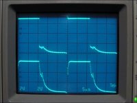
from pads 1 to 3 of the FETs


when I feed the scope a 1k square wave with a wave generator, it just looks like a sine wave with squared off tops, like the first pic, and I see the same spike show up like in the second pic (which is what I believe is for only ignition/spark events)
when I feed the scope a 1k square wave with a wave generator, it just looks like a sine wave with squared off tops, like the first pic, and I see the same spike show up like in the second pic (which is what I believe is for only ignition/spark events)
Last edited:
- Status
- This old topic is closed. If you want to reopen this topic, contact a moderator using the "Report Post" button.
- Home
- General Interest
- Car Audio
- Digital Designs M2a Repairs in process