Does anyone know where I can get a schematic or service manual for
Precision Power PC2350?
.... Thanks in advance..
e-mail: staykov1975@abv.bg
Precision Power PC2350?
.... Thanks in advance..
e-mail: staykov1975@abv.bg
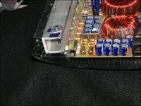
http://img193.imageshack.us/img193/9430/p1020446t.jpg
may be the problem is somewhere here...
may be the problem is somewhere here...
There are a couple of 2 pin headers in the audio section near the outputs. Place shunts on them and power up the amp. If it still makes noise or draws excessive, measure the DC voltage across the emitter resistors. If either channel has more than 0.000v across any of the emitter resistors, you have a problem in that channel. If it's drawing enough current to damage the power supply components, insert a 1-2 ohm resistor in series with the B+ line to limit the current. Of course, you should have the power semiconductors tightly clamped to the heatsink when doing this.
The whole storry is that:
1. We powered the amp with proper power sypply from 12 v accu, with 60 amp. fuse. We connet then remote pin to 12v DC. No load and input signal at the moment. All was ok. Outputs was 0.0v.
After that I applied 1KHz sine wave with small level, and I saw the output sine wave. The amp was ok in this moment.
2. I swithed off the amp and connect the load resistor 4 ohms 40W cooled by water.
3. Then we powered up again the amp, and slowly rising up input level up to point, when output was clipped. (this was approx. 36v RMS out voltage (around 325W).). This was done for less than 30 second, because we use small accu.).
4. After that we make some other measurements, and suddenly i hear some noise from PSU, and then I stopped immediately the supply from accu.
...(sorry for bad english") )
)
1. We powered the amp with proper power sypply from 12 v accu, with 60 amp. fuse. We connet then remote pin to 12v DC. No load and input signal at the moment. All was ok. Outputs was 0.0v.
After that I applied 1KHz sine wave with small level, and I saw the output sine wave. The amp was ok in this moment.
2. I swithed off the amp and connect the load resistor 4 ohms 40W cooled by water.
3. Then we powered up again the amp, and slowly rising up input level up to point, when output was clipped. (this was approx. 36v RMS out voltage (around 325W).). This was done for less than 30 second, because we use small accu.).
4. After that we make some other measurements, and suddenly i hear some noise from PSU, and then I stopped immediately the supply from accu.
...(sorry for bad english
)... cont..
5. I checked the power transistors, and i found 1 (2SA1303) that was defective. (short between BE and CE I think).
6. I replaced this transistor with new one, and checked everythink I can (All power transistors, incl 2 drivers (2SD2400 and 2SBxxx i think.) and other 2 poewers near ceramic modules. All was ok.
7 I powered Up the amp again for 1-2 secs (with no load), but the same storry. No w burned one transistor from other rail - 2scxxxx.
8. I replaced this transistor, and I checked all transistors again. All was ok.
9 Now, I connedted 1ohm/40W resistor on the positive power from the accu. (I know so the proper place is between PSU an Power Amp, but I don't want to cut some tracks and so...)
10. I powered the Amp again for short time, I hear againg noise from PSU, and swithed off. Now All output transisotrs was Ok, but there is steel some problem.
I think there is something wrong outside output stage. I measured BE resistors, and was ok. I tryed to draw the output part of the schematic to be more easy to find the problem, beacuse you know, without service manual or schematic it's not so easy ... The real problem is, so some stage before power transistors switching on both set output transistors in the same time, and this shorts power supply (and some of power transistors burning then).
About the current without load and input, when the amp was ok, I didn't measure is, but I think is was fine. (somewhere I read, that the whole current should be 3 amps...). Now, I can't measure, because the output stage shorts the power supply.
Today, I thinkd to make some other thing... To remove all power transistors from defective channel, and then to see if PSU and other channel is ok. But I thing PSU and other channel are good.
Our mistake was, so we put the amp in max power (around 330W on 4ohms load (one channel only), continous sine wave 1KHz), but this was done when the bottom cover was removed. This cover is not only cover, but it forces the transistors to be connected firmly to the heatsink. I checked transistors before to apply power voltage to be stuck to the heatsink, but probably some of them was not good connected to heatsink, and this was the reason, one of them to burn (thermaly, not by short cirquit ot other stupid thinks).
Tomorrow when I go to work, I'll check that you write (for 2 pin headers), and will try to take other part of scheamtic to see the reason for this problem.
Nice clamp bars Perry.I think I will make a set like that. I use flat bars currently.
And you are correct this amp can not be tested like they did without having the power devices clamped down tightly. Just way too much juice in this amp for that sort of stuff without adequate sinking for the power transistor's.
Lucky they did not fail the lower rail supply pass elements along with the couple outputs... The lower rail supply pass transistors run hot at idle without a load, as I am sure you already know.
Also don't forget to measure the voltage drop across each emitter resistor set to check for poorly matched outputs due to replacement, which could cause uneven current sharing and output failure again after its all buttoned up...At this voltage level output matching is pretty much a must do for reliability reasons IMO&E...
Today I have some success with this amplifier, but it seems strange, there is no quiescent bias current on power transistors. Somewhere I read, so this amp is class AB, but there are no voltage (or less than 1mv) drop on the 0.33ohm pairs resistors on emitters of the power transistors. It seems to be Class B, or I measured something wrong, because I do this in last moment before to go. The potentiometers are not touched by me. First one is for output “0” correction I thing, and the second one (R90) is for quiescent bias current. (I measure all this with no load, no input signal, and jumpers JP1 and JP2 open).
BTW, I removed all output power transistors (2SA1303 and 2SC3284) from the channel, that I think is bad, and then I applied the power from accu, and when I checked quickly output PSU voltages (+/- 56v), and no output DC voltage on outs, I connected audio in to 1KHz small sine signal, and both outputs was OK. (The channel without Power transistors still can work, if it is without load because Q20 and Q22 are still there.). After this test, I soldered 1 pair (PNP and NPN) power transistors to this channel, and checked again (without load of course) and again all was ok. So, I think Monday, when I connect All other transistors, all should be fine. Only I have to solve the problem with quiescent bias current and to check if all transistors in to the same rail are with similar parameters (but this can be done, if there is some quiescent bias current).
Total current drain from 12V power is 2 Amps (I think it should be 3 Amps.), but real voltage on my accu is 11.2v .
Perry can also verify this tidbit. The jumper located in the middle of each channel is to be jumper-ed so to bypass the thermal sensing so a steady bias setting can be achieved at room temperature and not have the temperature variance cause it to drift all over the place while you making final adjustments.
I myself am unsure of a factory bias point based on voltage drop across the emitter resistors, but I like to scope my amps to set this as to avoid crossover notch distortion, while staying within the Idle current draw spec from the amp maker, and keeping both channels as closely matched as possible.
Also be on the look out for the other adjustment pots in the channel that are for DC offset at the output.
These will also drift with bias a bit, so you will be going back and forth between these set points a bit until you find the sweet spot this amp likes to play at.
Been there and done this many times....
So, This amplifier seems to be typical Calss B. No diodes like AB Class amps, Ube of the power transistors is 170mV --> no quiescent bias current , transistors are off. If someone have original (not repaired or tuned) and can measure quiescent bias current of power transistors, and if is more than 0 ---> please share with us
Driver board is suppyed with +/-56v and power transistors with +/-58..59v.
Actualy, I can force to bias output stage with 6-7mA per transistor ot little bit more(with potentiometer R90 - in thermal compensation part), but the interesting thing for me is, so I newer touched both potentiometers , and the one channel, that I never repaired, have zero bias too. ( But I'm not sure if someone other is changed value of this potentiometers or not)
I'll try to put bias current on the output stage, but then I have to test the amp in High temperature mode... to see if the thermo compensation cirquit works well.
And one think more... I see one of the power transistors was replaced before... Now I replaced two more. I have measured h21e on all transistors (both rails), and see 10-15% difference between them. I know it's better to be as much as possible the same, but how much is enough?
Perry can also verify this tidbit. The jumper located in the middle of each channel is to be jumper-ed so to bypass the thermal sensing so a steady bias setting can be achieved at room temperature and not have the temperature variance cause it to drift all over the place while you making final adjustments.
I myself am unsure of a factory bias point based on voltage drop across the emitter resistors, but I like to scope my amps to set this as to avoid crossover notch distortion, while staying within the Idle current draw spec from the amp maker, and keeping both channels as closely matched as possible.
Also be on the look out for the other adjustment pots in the channel that are for DC offset at the output.
These will also drift with bias a bit, so you will be going back and forth between these set points a bit until you find the sweet spot this amp likes to play at.
Been there and done this many times....
Hey all- Factory bias was set at .7V across the emitter resistors. You're method is probably better though.
As Perry mentioned, this amp can be biased without being attached to a HS, just keep an eye on the temperature of the voltage regulators on either side of the board. Under normal circumstances, these can be run for several minutes without being sunk.
- Status
- This old topic is closed. If you want to reopen this topic, contact a moderator using the "Report Post" button.
- Home
- General Interest
- Car Audio
- PPI PC2350 schematic or service manual??