This is my first time working on Car Amps and after reading everything I could find here I have a general idea how the things work but I could use some additional guidance.
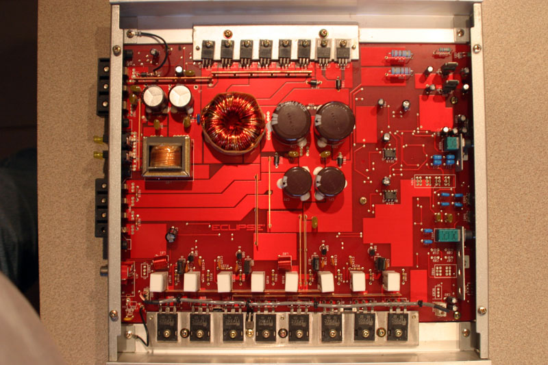
Here's what I'm working on.
Nothing is burned, it doesn't blow fuses, and nothing gets hot.
When apply +12v to the remote it will power up for a couple of seconds and then the SMPS will shutdown. It the short time that it's running I see the rails at +- 38v.
It uses a 494.
The switching MOSFETs are 6 S2K3057 and the diodes are a F12C10A and C.
I've checked all the semiconductors for shorts in circuit. I didn't want to unsolder them all until it proved to be needed.
I pulled the board out or the case to start tracing and measuring the pins on the 494 and when I power it up it stays running drawing about 800ma, the rails sit at +37.9v and -37.9v but there is a 3.39v DC offset on the right channel and virtually no DC in the left.
I've been focusing on the SMPS since it was shutting down.
Why does mounting it on the case make a difference?
Is is likely that the real problem is whatever is causing the DC on the right side? Where should I start looking to track that down?
There are more pictures at http://simon.chi.il.us/~steve/E33230
I don't have schematics, I've kind of worked my way through the SMPS circuit and haven't started looking at the audio side.
Thanks for any suggestions.
Here's what I'm working on.
An externally hosted image should be here but it was not working when we last tested it.
An externally hosted image should be here but it was not working when we last tested it.
Nothing is burned, it doesn't blow fuses, and nothing gets hot.
When apply +12v to the remote it will power up for a couple of seconds and then the SMPS will shutdown. It the short time that it's running I see the rails at +- 38v.
It uses a 494.
The switching MOSFETs are 6 S2K3057 and the diodes are a F12C10A and C.
I've checked all the semiconductors for shorts in circuit. I didn't want to unsolder them all until it proved to be needed.
I pulled the board out or the case to start tracing and measuring the pins on the 494 and when I power it up it stays running drawing about 800ma, the rails sit at +37.9v and -37.9v but there is a 3.39v DC offset on the right channel and virtually no DC in the left.
I've been focusing on the SMPS since it was shutting down.
Why does mounting it on the case make a difference?
Is is likely that the real problem is whatever is causing the DC on the right side? Where should I start looking to track that down?
There are more pictures at http://simon.chi.il.us/~steve/E33230
I don't have schematics, I've kind of worked my way through the SMPS circuit and haven't started looking at the audio side.
Thanks for any suggestions.
but there is a 3.39v DC offset on the right channel
There is your bad channel my friend. The DC offset is the clue. Try comparing the left channel to right channel with a ohm meter they should be mirror images of each other. I am sure you will find significantly different readings among the transistor somewhere in that bad channel when compared to the good channel....hope this helps.
PS your SMPS is working fine as its protecting the entire amp by shutting the amp down. So I would leave the power supply as good for now till the channel is debugged...
1moreamp said:
There is your bad channel my friend. The DC offset is the clue. Try comparing the left channel to right channel with a ohm meter they should be mirror images of each other. I am sure you will find significantly different readings among the transistor somewhere in that bad channel when compared to the good channel....hope this helps.
PS your SMPS is working fine as its protecting the entire amp by shutting the amp down. So I would leave the power supply as good for now till the channel is debugged...
Thanks, hopefully you could tell that I was starting to get the impression that was the cause of the shutdown but I'm still confused as to why removing the case changed the behavior. I'm glad it did because I wouldn't have been able to discover the offset issue since it didn't run long enough otherwise.
I'll sit down and trace out the circuit and then start measuring.
Do problems like this tend to be from bad discreet parts or transistor failures?
Yeah i've seen similar issues before like this. The DC offset may be causing different issues once the sink is removed , like thermal runaway for possible starters. So out of sink can be different then in sink just because of no thermal sink on the components being incorrectly driven. Such conditions could cause over current conditions to be passed to otherwise good devices.
I recommend that you tech the amp only mounted properly in the sink till its figured out. If not you might just cause more failure related issues.
By teching I mean remount the amp and then ohm out all the semiconductors in the known good channel as opposed to the known bad channel.
This is a good start, and use a marks-alot marker to place a dot were readings seem to be different in the bad channel. this should localize your area of repair.
Remember that these sort of amps are "Direct coupled" that means any bad transistor you find will be directly connected to another device that may or may not be bad. But it will read different because of the other failed device that connected to it. Its also a fair chance that the surrounding devices have been damaged by just one or two devices
If you get swamped, a sideways approach is to remove the outputs in the bad channel marking there location for reinstall later.
Then the amp should turn on without shutting down because there is no drive section connected to the output and therefore there will be NO 3.39 volts offset sent to the protection circuitry to shut the amp down. Then you can do live tech work... Hope this hint helps, been where you are many times...")
I recommend that you tech the amp only mounted properly in the sink till its figured out. If not you might just cause more failure related issues.
By teching I mean remount the amp and then ohm out all the semiconductors in the known good channel as opposed to the known bad channel.
This is a good start, and use a marks-alot marker to place a dot were readings seem to be different in the bad channel. this should localize your area of repair.
Remember that these sort of amps are "Direct coupled" that means any bad transistor you find will be directly connected to another device that may or may not be bad. But it will read different because of the other failed device that connected to it. Its also a fair chance that the surrounding devices have been damaged by just one or two devices
If you get swamped, a sideways approach is to remove the outputs in the bad channel marking there location for reinstall later.
Then the amp should turn on without shutting down because there is no drive section connected to the output and therefore there will be NO 3.39 volts offset sent to the protection circuitry to shut the amp down. Then you can do live tech work... Hope this hint helps, been where you are many times...
The amp could have bad solder joints somewhere on the board. When you removed the amp from the heat sink, the board may have flexed in a way that the bad joint is now making contact. As long as you are removing the board and you are leaving the transistors mounted to the aluminum strips, you should be able to power the amp up for a short time (30 seconds or so) without causing any damage. Just remember to check the strips for heat periodically. Put a single 10 amp fuse in the amp.
How did the behavior change in/out of the sink?
Set your meter to DC volts and connect the black meter probe to one of the non-bridging speaker terminals. Probe each of the pins of the two 8-pin op-amps and post the voltages (16 total).
IC 13
Pin 1:
Pin 2: ...
IC 14
Pin 1:
Pin 2: ...
Set your meter to DC volts and connect the black meter probe to one of the non-bridging speaker terminals. Probe each of the pins of the two 8-pin op-amps and post the voltages (16 total).
IC 13
Pin 1:
Pin 2: ...
IC 14
Pin 1:
Pin 2: ...
I Am An Idiot said:As long as you are removing the board and you are leaving the transistors mounted to the aluminum strips, you should be able to power the amp up for a short time (30 seconds or so) without causing any damage.
The key part of that transmission was the part about leaving the transistors mounted to the aluminum strips. Just wanted to make sure you saw that part.
1moreamp said:The DC offset may be causing different issues once the sink is removed , like thermal runaway for possible starters. So out of sink can be different then in sink just because of no thermal sink on the components being incorrectly driven. Such conditions could cause over current conditions to be passed to otherwise good devices.
I'm not taking the "all" the heat sinks off. You'll note that the devices on each side are all mounted to one AL strip which is in turn mounted to the chassis which is a huge AL extrusion. There is no sign of thermal runaway in or out of the chassis.
I Am An Idiot said:The amp could have bad solder joints somewhere on the board. When you removed the amp from the heat sink, the board may have flexed in a way that the bad joint is now making contact. As long as you are removing the board and you are leaving the transistors mounted to the aluminum strips, you should be able to power the amp up for a short time (30 seconds or so) without causing any damage. Just remember to check the strips for heat periodically. Put a single 10 amp fuse in the amp.
I've checked the board for bad solder joints and resoldered anything that looked the least bit questionable. It's possible there is one but I didn't see anything. With all the SMD parts I need to take another look with the magnifier. I'll also try not using the screws going through the board to the chassis and see it that changes anything.
The lab supply I use has current limiting enabled. It helps cut down on releasing the magic smoke. Once I'm sure it's not going to burn up I'll switch to a fused high current source.
Yes, the MOSFETS, diodes and BJT outputs are all mounted to the strips and they are not heating up. The amp inputs are floating. If I start probing signal paths should I short them?
Perry Babin said:How did the behavior change in/out of the sink?
Set your meter to DC volts and connect the black meter probe to one of the non-bridging speaker terminals. Probe each of the pins of the two 8-pin op-amps and post the voltages (16 total).
Perry, I'll post the voltages at the op-amps when I go back into the basement. BTW they are JRC 318D's.
The behavior was that the SMPS shut down after about two seconds when mounted normally. Once free of the chassis it stays running and idles along at about 800ma input current @ 13.6v but with the DC offset on the right channel.
I'm not sure what the correct terms are for the rest of the transistors but the first stage are a complementry pair of 2SC2705/2SA1145, the drivers are 2SB1186A/2SD1763A, and the outputs are TIP35C/TIP36C
Thank you all for your input.
Since I can't edit my posts could a moderator fix the second image link to this. (I intended to post it and not two copies of the top)
An externally hosted image should be here but it was not working when we last tested it.
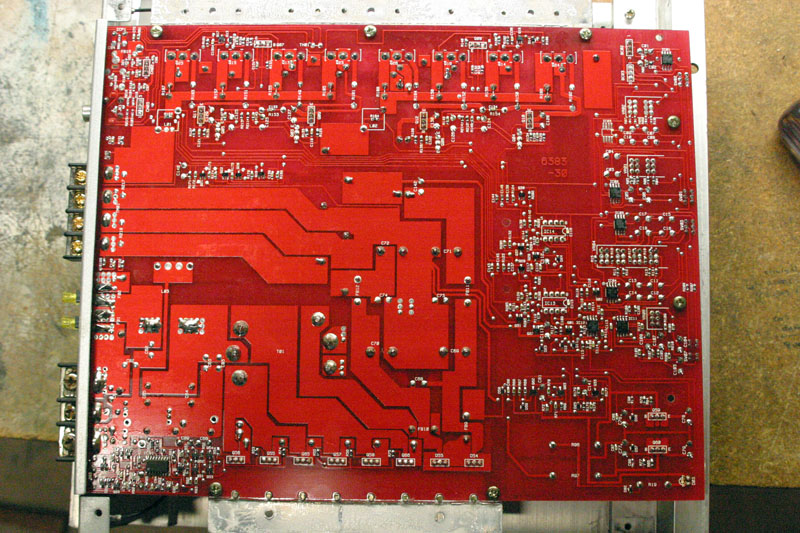
OK then check to see if there is any DC voltage on the aluminum where the power devices attach . Measure with respect to both grounds I.E. 12 volt ground and center tap of the toroid secondary side. If there voltage then you may have a bad insulator of a metal shaving , or what not causing a circuit where there should be none. Just thinking out load. I've seen a many a bad insulator over the years..
Perry Babin said:How did the behavior change in/out of the sink?
Set your meter to DC volts and connect the black meter probe to one of the non-bridging speaker terminals. Probe each of the pins of the two 8-pin op-amps and post the voltages (16 total).
Using the non-bridging common speaker terminals as ground.
IC 13 LM318
Pin 1: 13.46V
Pin 2: 1.8mV
Pin 3: -0.5mV
Pin 4: -15.97V
Pin 5: 13.63V
Pin 6: -3.4mV
Pin 7: 15.99V
Pin 8: -14.77V
IC 14 LM318
Pin 1: 13.48V
Pin 2: 3.381V
Pin 3: 3.392V
Pin 4: -15.98V
Pin 5: 13.64V
Pin 6: 224.8mV
Pin 7: 16.0V
Pin 8: -14.77V
I didn't get a chance to look at the voltages in front of the op-amps and see where the differences start.
1moreamp said:OK then check to see if there is any DC voltage on the aluminum where the power devices attach . Measure with respect to both grounds I.E. 12 volt ground and center tap of the toroid secondary side. If there voltage then you may have a bad insulator of a metal shaving , or what not causing a circuit where there should be none.
If I'm not too sleepy the center tap secondary is common with the two non-bridging speaker terminals.
The measurements to the two heatsinks and the non-bridging speaker terminals were millivolt range and climbed while measuring like when charging a cap.
What's confusing to me in my sleep deprived state is why I see a -18.5V difference between the center tap of the secondary and the 12V ground. I also see the same offset between the grounding wire on the transistor side of the circuit board and the grounding wire on the SMPS side of the board.
Should the audio signal ground and the chassis ground be that far apart?
As soon as I connect the two grounding wires the SMPS goes back to shutting down after a few seconds.
Sorry I'm just plodding here.
It appears that IC14 is being driven with 3v of DC. With your black probe on a non-bridging speaker terminal, measure the DC voltage on both terminals of C112 (near IC14). Post the voltage on each terminal.
The negative voltage MAY be the protection circuit trying to pull a transistor down to the -regulated voltage.
The negative voltage MAY be the protection circuit trying to pull a transistor down to the -regulated voltage.
Perry Babin said:It appears that IC14 is being driven with 3v of DC. With your black probe on a non-bridging speaker terminal, measure the DC voltage on both terminals of C112 (near IC14). Post the voltage on each terminal.
C112+ 3.36V
C112- 0v
I haven't finished tracing the circuits hanging off pins 2 and 3. From what I can tell the C112- should be at ground like it is.
All the the circuits going to pin 2 on the op-amp look like a feedback network since they go all the way back to the output transistors. I haven't figured out what Q28 and D24 do.
Analog circuits are what chased me into software so many years ago.
Perry Babin said:Post the voltages on IC12. It appears to be driving the positive (non-inverting) input of IC14.
I can't find datasheets for the 9038 or 9132 parts. I assume they are op-amps. The 9038's look like a dual op-amp of some sort. With pin 3 and 5 being the non-inverting inputs, 2 and 6 the inverting inputs and 1 and 7 the outputs. 8 and 4 look to be the V+ and V-.
I'd like to be more than a monkey with a voltmeter and have some idea what I'm looking at. Do you have them?
IC12 9038B
Pin 1: -0.2mV
Pin 2: -0.2mV
Pin 3: 0.7mV
Pin 4: -16.14V
Pin 5: 0v
Pin 6: -0.2mV
Pin 7: 14.13V
Pin 8: 16.07V
If the pinout above is correct I'd say this one is blown.
I HAD THE EXACT SAME ISSUE WITH MY ECLIPSE 33230 Here is what happened and what fixed it. Somehow the ground wire came loose and the amp began drawing current from the chassis ground, it then blew my speakers.
Afterwards I had the exact 38v DC output problem at the speaker terminals. Because of the mising ground lead EVERY DIODE in the amp fried, some fried open and some fried closed. There are 4 through-hole diodes in the amp section FB09, FB10, FB11 and FB12 and one at the chassis ground jumper FB15. Every one of those needed replaced and also needed to replace D56 and D57 that are surface mount diodes on the other side of the board in the preamp section right near the power light.
If you are having nearly the same problem such as this, start with testing/replacing these diodes and see what happens.
Thank you for the advice.
You'll note that I didn't have 38v DC output at the speaker terminals, I had 3.39v DC offset on the right channel. The power supply rails were at +- 38v like they should have been.
I had to set this aside back then to focus on other projects and it remains something to play with when I don't have anything else to do. When I do I'll keep in mind checking the diodes. FB09, FB10, FB11, FB12, FB15 are ferrite beads with a wire run through them not diodes. They're cemented I assume to keep them from rattling. On my amp they are all fine.
- Status
- This old topic is closed. If you want to reopen this topic, contact a moderator using the "Report Post" button.
- Home
- General Interest
- Car Audio
- Eclipse 33230 shutting down