Konnichiwa,
Coulda toldcha....
Here is what you WANT to do.
1) Set up the input as cascode, J-Fet to BJT.
2) Degenerate the J-Fet's source sufficiently that with 50mV RMS input the current shifted is linear.
3) Add the RIAA Network in parallel to the CCS used as DC load for the Cascode, the entire RIAA network is of the shunt type.
If you have enough gain in the cascode and enough supply voltage all you need after this circuit is a buffer, so it could be made "single-stage".
If you go 2-Stage anyway you can probably omit the CCS load and just use the RIAA Networks Shunt resistor (the 3180uS) to supply the supply current.
One might even conceive a "split EQ" version of this, with the 3180/318uS EQ in the Drain connection of the first stage and the 75uS in the second stage.
Using 2SK170BL with cascode gives around 10mA/V transconductance once degenerated, at a current in the 2-5mA range. If we select for around 4mA and use 3K3 as Load we need a 330R in series with around 1uF. The resultant gain @ 1KHz would be around 10db. We need a suitable shunt capacitor for the 75uS EQ, I'd expect around 330nF should work, best shunt this through some simulator, calculating networks by hand according to lipshitz is too hard work for me on a friday.
Then add a second stage with a higher current (and Gm) selection (say 10mA @ 30mA/V) and a 1K load. Done.
We did a somewhat "inbetween" this shunt EQ with cascode and the traditional EQ version of the l'Pacific. PSU via PP3 NIMH Cells X 3, Cascode BJT's from the first battery at around 8V, main supply around 24V. Worked great... I suspect the Shunt EQ would have been even better.
Sayonara
wrenchone said:The simulation results inducate that one should not be using an SRPP as the front end of a passively equalized RIAA amp.
Coulda toldcha....
Here is what you WANT to do.
1) Set up the input as cascode, J-Fet to BJT.
2) Degenerate the J-Fet's source sufficiently that with 50mV RMS input the current shifted is linear.
3) Add the RIAA Network in parallel to the CCS used as DC load for the Cascode, the entire RIAA network is of the shunt type.
If you have enough gain in the cascode and enough supply voltage all you need after this circuit is a buffer, so it could be made "single-stage".
If you go 2-Stage anyway you can probably omit the CCS load and just use the RIAA Networks Shunt resistor (the 3180uS) to supply the supply current.
One might even conceive a "split EQ" version of this, with the 3180/318uS EQ in the Drain connection of the first stage and the 75uS in the second stage.
Using 2SK170BL with cascode gives around 10mA/V transconductance once degenerated, at a current in the 2-5mA range. If we select for around 4mA and use 3K3 as Load we need a 330R in series with around 1uF. The resultant gain @ 1KHz would be around 10db. We need a suitable shunt capacitor for the 75uS EQ, I'd expect around 330nF should work, best shunt this through some simulator, calculating networks by hand according to lipshitz is too hard work for me on a friday.
Then add a second stage with a higher current (and Gm) selection (say 10mA @ 30mA/V) and a 1K load. Done.
We did a somewhat "inbetween" this shunt EQ with cascode and the traditional EQ version of the l'Pacific. PSU via PP3 NIMH Cells X 3, Cascode BJT's from the first battery at around 8V, main supply around 24V. Worked great... I suspect the Shunt EQ would have been even better.
Sayonara
KYW - been there, done that (well, sorta). See my thread called "Open Loop Follies". The RIAA preamp I just replaced had a cascoded 2SK170GR front end with a current source loaded source follower (circuit (1) shown earlier in this thread). I used a JFET cascode, though. The circuits are in the cited thread. I don't really have any problem with a simple common source amp at the input. The distortion is very small (<0.01%) for low level operation. My big concern was with the second stage, which had about 0.4% distortion for about 1V output using the same type of gain cell. The distortion is overwhelmingly 2nd order, but it irks me none the less. This distortion level seems unavoidable wih a simple common source open loop amp, cascoded or not. Using the SRPP was an attempt to get around the high level distortion at the second stage. I also wanted to see what it would take to get one to work, as an earlier attempt at an SRPP preamp using JFETs was unsuccessful.
For a passive equalized RIAA amp, I like to split the gain in two pieces, usually with a gain of about 40 on the first stage and 30 for the second stage. This gives me aroound 40 dB gain at 1kHz, which is right about what my system wants to see. I wouldnt feel too comfortable putting all the gain in the first stage.
I'm also fairly adamant these days about using readily available devices (in the US, at least) in my recent circuits, especially after the fulminations from some pundits that insist that the only way to get decent sound is to use a 2SK170 or the like. I don't have anything against these devices (I have them, like them, and have used them), but I don't like absoute statements like that, especially without any real supporting data (and, may I add, contrary to my experience).
The next pass will most likely have a common source amp with cascoding (JFET) and degeneration driving a current souce loaded source follower. With even the fairly lowly PN4393, you can get a follower with ~50 ohms output impedance or less. This helps to get around any effects of output impedance on RIAA accuracy. I will also sum a current source into the drain of the gain FET (circuit (3) shown earlier in this thread). Adding the current source allows one to use high IDSS devices like the PN4393 or J110 without excessive degeneration, and still be able to adjust for optimum gain and voltage centering at the output. Since the gain FET runs with more bias current, the distortion is lower, and the cascoding keeps the FET from running too hot.
I'm thinking of still using an SRPP for the second stage with an optimized capacitively coupled load resistor, followed by another current source loaded source follower.
These topologies will allow me to build the preamp with JFETs I can order straight from Mouser and/or Electronic Goldmine.
For the correspondent that was asking about the rationale behind the output connection on the circuit, do a seach for SRPP on Google. You'll get a lot of information about the theory behind the SRPP (the Tube Cad article is especially good), which is a poor man's push-pull with gain. Most of the discussion will focus on tube applications. If you shift the output connection to the drain of the bottom FET, you get a common source amp with current source loading, an entirely different beast (I'm working on one of those with global feedback for a line amp application - yet another thread).
Well, I originally set out to do a preamp with a cascoded JFET common cathode for first stage and an SRPP for the second stage (the boards are (9/10 stuffed), but some recent simulation results made me lay these boards aside to try something different.
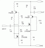
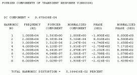
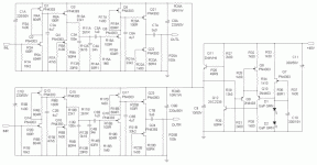
Attached is a schematic showing a MOSFET common source amplifier with cascode and a current source to bias up the MOSFET without all the bias current going through the load resistor. I simulated one of these using a Zetex ZVN3306 (Orcad had the device model) for active device, and high level distortion (~2V out into a 20k load) was around 0.05%, overwhelmingly 2nd harmonic. This was without the benefit of an output buffer. Needless to say, I'm trying this circuit out for the second stage of my RIAA preamp. Once I have the boards up and running, I'll start a new thread. I'm using the Supertex VN0106N3 instead of the Zetex devices, as I have loads of them in my parts bin.
Attached is a schematic showing a MOSFET common source amplifier with cascode and a current source to bias up the MOSFET without all the bias current going through the load resistor. I simulated one of these using a Zetex ZVN3306 (Orcad had the device model) for active device, and high level distortion (~2V out into a 20k load) was around 0.05%, overwhelmingly 2nd harmonic. This was without the benefit of an output buffer. Needless to say, I'm trying this circuit out for the second stage of my RIAA preamp. Once I have the boards up and running, I'll start a new thread. I'm using the Supertex VN0106N3 instead of the Zetex devices, as I have loads of them in my parts bin.
Attachments
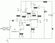
Funny you shoud ask - I screwed up, and there's an important piece missing out of the schematic I posted. There needs to be a second current source. The attached schemaitic is the one I used to do my simulation, and it has all the pieces...
M1 is the gain FET. M2 is used to set the overall bias current in M1. The ratios of R3 and R6 set the ratio of bias currents between M1 and M2. Ideally, one would use a current source in place of R10, and M1 and M2 would be matched and thermally coupled.
J1 is used to pin the drain voltage of M1. This provides the benefits of cascode operation, and also reduces the drain voltage of M1, reducing power dissipation and allowing use of a TO-92 device with relatively high bias current. The small device will need a lower bias current to get it into a "sweet" operating region. The small devices also have lower input capacitance.
Current source I1 is used to maintain the bias current in M1 without having it all flow through gain resistor R1. This allows one to have a greater range of choices for gain resistor R1 and still be able to center the output voltage near 1/2 the supply voltage for maximum symmetric output swing.
Since most of the bias current for M1 flows through current source I1, the power dissipation in J1 is relatively small. Also, since the voltage across I1 is pretty much constant, one can place a resistor in series with it to limit the power dissipation in whatever real-world device is actually used.
I suspect that most of the benefits of this topology are derived from operating M1 at a relatively high value of bias current, so that the signal current is a relatively small fraction of the bias current. The high bas current in M1 also places it in a more linear operating region.
Attachments
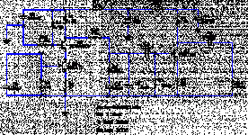
I've done a little more looking at the JFET SRPP preamp circuit, which caused me to revive this thread. A possible solution to the variable gain caused by the variable load presented to the first stage SRPP by the passive equalization network is to use a capacitively coupled fixed load, followed by a buffer.
For some reason, I didn't try that approach when this thread was more alive. Some recent simulations showed that the approach had promise, so I hacked an older board into shape using the circuit shown below. Simulations seemed to indicate that one could get by with a DC coupled fixed load on the SRPP stages to define a fixed gain. In practice, a cacacitively coupled load is needed so as not to disturb the DC balance of the SRPP stages. The SRPP stages used PN4303 JFETs (National) matched for VGS at 2 mA drain current. The output buffers are PN4393 loosely selected for drain current of ~ 10 mA.
This circuit will go into my living room preamp test bed for listening tests. If I like it, it may go to Burning Amp with me this year.
Attachments
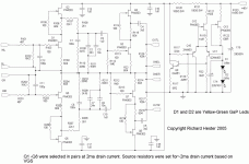
The circuit I just showed was the old circuit - let me see if I can select the new one instead. All the comments in the last post apply - this one is the real deal. What is ahown is two channels of RIAA with a common regulated supply. I'd like to point out that the gain is optimized for MM or high output MC cartridges.
Attachments
Very nice solutions. Now the SRPP loses its Achilles heel. Should perform at its best. More fets are more fets though, and the sonic tests will let you know what weighs more in this circuit. Please let us know more when practically ready and testing. Best of luck with this sophisticated and most original phono!
 .
.The 16k input resistor is optimized to damp out the ultrasonic peak in the response of my Grado gold cartridge. I didn't add any input capacitor for the reason you suggest - that there is already some from the input cables. The Grado cartridges are relatively insensitive in that regard - the data sheet does not even bother to specify an optimum load capacitance. There will also be Miller capacitance from the input JFET. The PN4303 is a reall lightweight in that regard, having an input capacitance of 6 pF, and a reverse transfer capacitance of 3 pF.
The PN4303 is only in current production from Fairchild, as far as I can tell. I've been using NOS devices from National, who divested their small signal lineup a long time ago. I wish I could get some of the Vishay/Siliconix parts, but they discontinued the 4303 a couple of years ago, and have recently killed just about all their JFET line. The problem with the Fairchild version of the part is that the data sheet rather grudgingly admits that the part is a JFET and has three legs, and that's about all. Noise is not mentioned. They may work just fine, but they may also hiss like vipers. Having said that, I have some of the recent Fairchild parts, and will try them when I get a chance. I also scored some 2N4303s from Amelco (the orignal version of this part) - real museum pieces in a TO-106 package. I'm really interested to see how they work out.
A reasonable substitute for the 4303 may be the J202 - the specs are similar, and the noise is ok, though not as low as the PN4303.
OK
The problem with this design and allmost everyone else is that I can't get hands on the components you suggest. Everyone want something at the edge or may I say difficult and "hard to do design".
If I just try 2SK170GR or 2SK117 which I easily can get?
The aftersought shimmering is gone? Distortion figures bad?
Schematic looks good of your design.
About noisy FET's I remember my younger days when we copied the layout of a MXR phase 90 pedal (effectpedal for guitars)
Sometimes it went for a while but eventually it got noisy from some of the FET's. I even did a similar effect from the magazine Practical electronics. Beautiful sound.... until the FET's started to bring in "rain and wind". I think I used the workhorse BF245 in both designs.
I understand you have to handpick FET's more troughly then other transistors?
For MM cartridges, FETs with about 1-1.5 mS transconductance are about right., and even these are a little hot... 2SK170s have way, way too much gain for the application,. Just for grins, I tried a pair in simulation, and the high end starts sagging at about 3 kHz (plus the gain is way too much, but not enough for a single stage). You want to spread out the gain between two stages anyway - its a compromise between distortion and dynamic range.
Appropriate FETS - PN/2N 4303, J202. Both of these have good drain voltage rating (40V) and the right gain. The 2N5457 and 2N5458 will work, but as their breakdown voltage is only 25V, the dynamic range will suffer.
If you insist on using something like a 2SK170, pass on this circuit and try something based on a simple common emitter amp, like the Pacific. One useful frill ifor the Pacific is adding a cascode to reduce the capacitive load on the cartrige from Mr. Miller. Another frill is adding a source follower to the front end so that you have a low (and more or less invariant) impedance driving the passive RIAA network a source follower after the output stage adds peace of mind for driving output cables. . Check my thread "Open Loop Follies" for more on this, as well as the "All American" thread for another approach.
What about this one? Good to drive down to 40k line in preamp loads, or it can take another stage, a simple source follower in its tail for more demanding loads. Can tap off from added source follower's input and have 2 outputs. One buffered, one non.
Attachments
wrenchone said:
If you insist on using something like a 2SK170, pass on this circuit and try something based on a simple common emitter amp, like the Pacific. One useful frill ifor the Pacific is adding a cascode to reduce the capacitive load on the cartrige from Mr. Miller. Another frill is adding a source follower to the front end so that you have a low (and more or less invariant) impedance driving the passive RIAA network a source follower after the output stage adds peace of mind for driving output cables. . Check my thread "Open Loop Follies" for more on this, as well as the "All American" thread for another approach.
P.S.
The above circuit I posted ties with your quoted paragraph, that I assume was answering to Radioman62 wanting to use 2SKs. I did not post it as having anything to do with your SRPP concept. Its an example of what you say in that paragraph I hope.
salas said:What about this one? Good to drive down to 40k line in preamp loads, or it can take another stage, a simple source follower in its tail for more demanding loads. Can tap off from added source follower's input and have 2 outputs. One buffered, one non.
That looks like something to try before going for the more complex amplifiers.
Hmm.. If I only had some more sparetime
")
- Home
- Source & Line
- Analogue Source
- JFET SRPP RIAA Preamp