I can find the Zin of a JFET as either 50Meg or 100Meg, on the 'net.
However, when you use a pair of JFETs ... does this make the Zin half (in the same way as a parallel pair of equal-value resistors has a value of half the individual value)?
So a pair of JFETs has a Zin of 25Meg or 50Meg?
Anybody know.
Thanks,
Andy
However, when you use a pair of JFETs ... does this make the Zin half (in the same way as a parallel pair of equal-value resistors has a value of half the individual value)?
So a pair of JFETs has a Zin of 25Meg or 50Meg?
Anybody know.
Thanks,
Andy
onnected
Yes, when connected in parallel, the net input impedance is cut in half. Keep in mind that FETs can have significant input capacitance, which iwould be doubled, just as it would be if connecting two equal value capacitors in parallel. It is the the capacitive reactance which is then cut in half.
Yes, when connected in parallel, the net input impedance is cut in half. Keep in mind that FETs can have significant input capacitance, which iwould be doubled, just as it would be if connecting two equal value capacitors in parallel. It is the the capacitive reactance which is then cut in half.
Last edited:
Yes, when connected in parallel, the impedance is cut in half. The capacitive reactance is cut in half, which means the input capacitance is doubled. Just as it would be when connecting two equal value capacitors in parallel.
Thanks very much, Ken.
Given I now have to halve the Zin (and even quarter it, in one circuit implementation, as I use a matched quad of JFETs), the combined Zin becomes important.
What do you suggest (given I've found both values on the 'net) for the Zin of a single JFET - should I take it as 50Meg ... or 100Meg?
And thanks for the additional info on capacitance - which I hadn't considered!
 This means I need to take the Miller capacitance of the 2nd stage of my circuit as twice (or four times) what I had calculated it to be! (This affects cap values in the RIAA circuit which preceeds the 2nd gain stage.)
Andy
Do you connect them in parallel or in anti-series, that is, as a differential pair?
To determine the Zin of a JFET at very low frequencies, you need to know how gate current varies with gate-source voltage around the bias point you choose. If you are very lucky you may find that in a graph in the datasheet, but it is more likely that you don't. At all but the very lowest frequencies the capacitances dominate.
To determine the Zin of a JFET at very low frequencies, you need to know how gate current varies with gate-source voltage around the bias point you choose. If you are very lucky you may find that in a graph in the datasheet, but it is more likely that you don't. At all but the very lowest frequencies the capacitances dominate.
Do you connect them in parallel or in anti-series, that is, as a differential pair?
In parallel, Marcel. Does that make a difference?
To determine the Zin of a JFET at very low frequencies, you need to know how gate current varies with gate-source voltage around the bias point you choose. If you are very lucky you may find that in a graph in the datasheet, but it is more likely that you don't. At all but the very lowest frequencies the capacitances dominate.
Sorry, don't quite get what you are saying??
Are you sayng that Zin of a JFET varies with frequency?
Andy
Connecting them in anti-series would increase rather than decrease the impedance (as well as the noise voltage).
The input impedance consists of a resistive part in parallel with a capacitive part. The impedance of the capacitive part is inversely proportional to frequency.
The input impedance consists of a resistive part in parallel with a capacitive part. The impedance of the capacitive part is inversely proportional to frequency.
The input impedance consists of a resistive part in parallel with a capacitive part. The impedance of the capacitative part is inversely proportional to frequency.
Thanks, Marcel - understood.
Andy
How high impedance do u need? I wouldn't use the JFETs inputZ as design parameter but rather a gate to gnd resistance that dominates at all temp and frequencies. You might wanna google jfet gate leakeage current. If going to use much larger than 1megohm I'd select JFETs with specified low leakeage. If drift and uncertain Zin is not so critical u can of course use much higher resistance.
Do u want to go that high in a phono pre? Even if in the second gain stage it may be nice to keep resistance reasonable to keep noise down.
Do u want to go that high in a phono pre? Even if in the second gain stage it may be nice to keep resistance reasonable to keep noise down.
The low frequency input resistance of a JFET probably varies by a ratio of 10:1 between different samples, so who cares that paralleling two of them halves a value you don't know at all accurately anyway? Your circuit should not assume any particular value, but merely assume that it will be high and presumably swamped by other circuit components.andyr said:I can find the Zin of a JFET as either 50Meg or 100Meg, on the 'net.
No, he is saying that Zin varies with bias point. In addition, there will be capacitance (both gate and Miller) which may vary with bias and its reactance will of course vary with frequency too. The net result is that at higher frequencies the input impedance of a JFET is mainly capacitive - you can ignore the resistance (which you didn't know the value of anyway).Are you sayng that Zin of a JFET varies with frequency?
The low frequency input resistance of a JFET probably varies by a ratio of 10:1 between different samples, so who cares that paralleling two of them halves a value you don't know at all accurately anyway? Your circuit should not assume any particular value, but merely assume that it will be high and presumably swamped by other circuit components.
I think it's a good question, though, because you can only ensure it is swamped by other components when you have at least a worst-case value for the resistance. For example, when you know it is between 100 Mohm and infinity and you want to make a 1 % accurate RIAA amplifier with passive correction, you know that the resistance of the RIAA correction network has to be smaller than 2 Mohm.
No, he is saying that Zin varies with bias point.
I neither said nor wrote nor meant that, but it is true of course.
Andy, to make the whole discussion a bit less abstract, could you tell us what type of FET, what drain current and what drain-source voltage you intend to use? We can then look in the datasheet to see whether there is anything specified in there that answers your question.
I think it's a good question, though, because you can only ensure it is swamped by other components when you have at least a worst-case value for the resistance. For example, when you know it is between 100 Mohm and infinity and you want to make a 1 % accurate RIAA amplifier with passive correction, you know that the resistance of the RIAA correction network has to be smaller than 2 Mohm.
Thank you, Marcel! My problem is that the equations to work out the correct values for a passive RIAA network incorporate the value of the gate-to-ground resistor which is just before the gain stage (which is after the passive RIAA network). And as the Zin of the JFET gain stage is in parallel with the gate-to-ground resistor ... it changes the value of that resistor.
Furthermore, when I use:
* a pair of JFETs, for lower noise, the Zin halves
* a quad of JFETs (for more gain), it quarters!
The fact that it can vary tenfold, as DF96 posted, between different samples is a further complication.
Andy
Andy, to make the whole discussion a bit less abstract, could you tell us what type of FET, what drain current and what drain-source voltage you intend to use? We can then look in the datasheet to see whether there is anything specified in there that answers your question.
2SK170, Marcel:
* drain current ~5ma
* drain-source voltage ~12v.
Andy
Cascading the Fet´s with bipolar transistors reduces the input capacitance.
Thank you, Joachim. Does it merely 'reduce' the capacitance ... or does it take it to zero?
Yes, I am aware of that - just not sure, when I have a CCS "on top of" the JFET gain stage, feeding current to the Drains (and enabling me to adjust Drain voltage), how I would fit a cascode transistor in there?
BTW, you are the guy who measured my long-time friend Hugh Dean's "Paris" headamp at -142dB SNR, are you not?
Andy
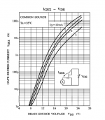
There is an interesting graph at the end of the datasheet that shows you that around your bias point, gate leakage increases by about 100 pA per 0.5 V of DRAIN-SOURCE voltage. That's equivalent to having a resistance of 5 Gohm between drain and gate. Similar to the Miller effect, you can calculate an equivalent between gate and source that is voltage gain of the stage plus one times smaller. So:
Per 2SK170: 5 Gohm/(gain of the second stage + 1)
For four in parallel: 1.25 Gohm/(gain of the second stage + 1)
As was already mentioned, this resistance is very inaccurate and non-linear. With cascoding, you can get rid of the "gain of the second stage" term, if you like.
Per 2SK170: 5 Gohm/(gain of the second stage + 1)
For four in parallel: 1.25 Gohm/(gain of the second stage + 1)
As was already mentioned, this resistance is very inaccurate and non-linear. With cascoding, you can get rid of the "gain of the second stage" term, if you like.
Attachments
If your RIAA values are sufficiently high that the JFET input impedance is a significant factor then you are likely to have problems with thermal noise.andyr said:My problem is that the equations to work out the correct values for a passive RIAA network incorporate the value of the gate-to-ground resistor which is just before the gain stage (which is after the passive RIAA network). And as the Zin of the JFET gain stage is in parallel with the gate-to-ground resistor ... it changes the value of that resistor.
There is an interesting graph at the end of the datasheet that shows you that around your bias point, gate leakage increases by about 100 pA per 0.5 V of DRAIN-SOURCE voltage. That's equivalent to having a resistance of 5 Gohm between drain and gate. Similar to the Miller effect, you can calculate an equivalent between gate and source that is voltage gain of the stage plus one times smaller. So:
Per 2SK170: 5 Gohm/(gain of the second stage + 1)
For four in parallel: 1.25 Gohm/(gain of the second stage + 1)
As was already mentioned, this resistance is very inaccurate and non-linear. With cascoding, you can get rid of the "gain of the second stage" term, if you like.
Thank you, Marcel - that graph didn't mean much to me!
OK, gain of the 2nd stage is 133 ... so your equations become:
* 1x 2SK170 - 37Meg Zin (not the 100Meg I had been assuming!), and
* 4x 2SK170 - 9Meg Zin!
Re. 'cascoding', if I send you the circuit diagram, can you tell me how to introduce a cascode ... so as to remove the '133' divisor?
Regards,
Andy
If your RIAA values are sufficiently high that the JFET input impedance is a significant factor then you are likely to have problems with thermal noise.
That depends; for a given transconductance of the first stage, a higher impedance of the RIAA correction network means more gain and less thermal noise.
- Status
- This old topic is closed. If you want to reopen this topic, contact a moderator using the "Report Post" button.
- Home
- Source & Line
- Analogue Source
- Zin of the 2nd stage of a JFET-based phono stage when a pair of JFETs is used?