A typical phono cart impedance was 47K, which means anything above 470K, and for sure 4.7Meg is irrelevant. A slightly higher input load resistor (47K+) compensates for any load from the FET. And the cable will have about 200pF capacitance, so again, the FET capacitance is irrelevant. Moving coil cartridges were much lower impedance, 50 to 100 Ohms, so the issue is worse, ie you needed a low-Z input that gives you the best S/N and distortion, not the highest impedance. The only time Hi-Z was important was with real cheap piezo cartridges, and they were never hi-fi. BTW, if a (47K) phono cart did not see the expected ~47K+200pF, it created a peaked response, however this and the effects of poor RIAA matching are what most vinyl fan love. Like guitar amplifiers, pure fidelity is not the objective.
A typical phono cart impedance was 47K, which means anything above 470K, and for sure 4.7Meg is irrelevant. A slightly higher input load resistor (47K+) compensates for any load from the FET. And the cable will have about 200pF capacitance, so again, the FET capacitance is irrelevant. Moving coil cartridges were much lower impedance, 50 to 100 Ohms, so the issue is worse, ie you needed a low-Z input that gives you the best S/N and distortion, not the highest impedance. The only time Hi-Z was important was with real cheap piezo cartridges, and they were never hi-fi. BTW, if a (47K) phono cart did not see the expected ~47K+200pF, it created a peaked response, however this and the effects of poor RIAA matching are what most vinyl fan love. Like guitar amplifiers, pure fidelity is not the objective.
Not quite sure what you’re getting at Steve?

If you’re saying that the value of R15 is wrong (at 47K) then what I didn’t tell you is that this is the default Zin, on the board - but I build it with parallel input RCAs, to take load plugs ... which bring down the Zin seen by the cart to whatever you want.
Andy
I think he means that the input impedance of the JFETs of the first stage is high enough to be neglected. For the resistive part he is absolutely correct (even though he seems to be confusing cartridge impedance and terminating impedance), for the capacitive part I'm not sure because of the Miller effect.
That is why you need to know exactly what the equations you have assume about things like source and load impedances etc.andyr said:My electronics knowledge is rudimentary ... I was relying on what a friend (who designs amps for a living) told me.
Unfortunately the component values for most RIAA networks all interact to set the required time constants, as well as the source and load resistances. It seems that while being unnecessarily concerned about the load resistance (511k in parallel with some JFETs) you largely missed the source impedance (2k in parallel with first stage output).
That is why you need to know exactly what the equations you have assumed about things like source and load impedances etc.
Understood.
It seems that while being unnecessarily concerned about the load resistance (511k in parallel with some JFETs) you largely missed the source impedance (2k in parallel with first stage output).
True, DF.
But googling 'JFET output impedance' brings up papers with some very heavy maths - which is completely beyond me. All I really need to know is whether or not the Zout of the 1st gain stage - with, say, a 2K 'gain resistor' between Drain and Ground - produces a substantially different result from the 2K I had assumed for the Drain res, in the RIAA calculations!
Andy
My guess is that it will produce a significantly different impedance. However, the total will still be somewhere between 0 and 2k, so when you add this to 47k you are talking about a variation of less than 5%. If you need to know more accurately than this then you either need to understand JFET gain stages well enough to calculate it, or measure the output impedance. I would go with measurement, as I expect the impedance to vary from one JFET sample to another - so you would get slightly different impedances on the two channels.
My guess is that it will produce a significantly different impedance. However, the total will still be somewhere between 0 and 2k, so when you add this to 47k you are talking about a variation of less than 5%. If you need to know more accurately than this then you either need to understand JFET gain stages well enough to calculate it, or measure the output impedance. I would go with measurement, as I expect the impedance to vary from one JFET sample to another - so you would get slightly different impedances on the two channels.
Thank you, DF. Very sensible advice.
But you're saying that if I set up a JFET with 12v on its Drain (and the 0v of the battery connected to Source) ... I could actually measure the Zout with my multimeter?
Then I would divide by either 2 or 4, depending on whether I had a pair of JFETs or a quad, in the 1st gain stage?
Andy
No. You need the slope or AC impedance, not the simple Ohm's Law DC impedance. It will vary with bias, and from sample to sample.
The way to measure it is to make an amplifer exactly like the first stage. Measure its voltage gain. Add an AC load (resistor plus coupling capacitor) to the output; measure gain again (across the resistor). Repeat a few times. The resistor value which halves gain is equal to the stage output impedance. Alternatively, you can plot a graph and read off the value.
The way to measure it is to make an amplifer exactly like the first stage. Measure its voltage gain. Add an AC load (resistor plus coupling capacitor) to the output; measure gain again (across the resistor). Repeat a few times. The resistor value which halves gain is equal to the stage output impedance. Alternatively, you can plot a graph and read off the value.
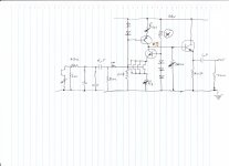
This is a version with an NPN cascode. The four extra diodes are supposed to be red LEDs. The 12v is now distributed more or less equally between the NPN and the JFETs, so the circuit can't handle large signals as well as it used to.
Hi Marcel
I have re-drawn the circuit with the changes you made - and I now understand it. Thanks.
Please see the jpg attached - have I drawn what you intended?
If so:
1. I presume that oblong box you drew between the 4x red LEDs (and the Base of the cascode transistor - NB: I drew only 3x LEDs) and the DC rail is a resistor?
2. what value res (which I marked as 'X')?
3. and that cascode transistor is a BC547C?
4. which could also be a BC550CG?
5. so what should 'V???' be set to (via the Rccs res)?
6. if I set it to 12v (1/2 DC supply) - which is what I set the Drain voltage to be, in the original circuit - then, as you said, 12v will be shared between the cascode transistor and the JFETs (so the JFETs will clip at 6 or 8v signal).
But how about setting 'V???' to, say, 16v (not 12v)? Then the JFET Drains will be at 8-12v ... so will have more headroom to cope with signal peaks?
Andy
Attachments
Last edited:
No. You need the slope or AC impedance, not the simple Ohm's Law DC impedance. It will vary with bias, and from sample to sample.
The way to measure it is to make an amplifer exactly like the first stage. Measure its voltage gain. Add an AC load (resistor plus coupling capacitor) to the output; measure gain again (across the resistor). Repeat a few times. The resistor value which halves gain is equal to the stage output impedance. Alternatively, you can plot a graph and read off the value.
Aah, OK.
Thanks, I will ponder this.
Andy
Hi Marcel
I have re-drawn the circuit with the changes you made - and I now understand it. Thanks.
Please see the jpg attached - have I drawn what you intended?
If so:
1. I presume that oblong box you drew between the 4x red LEDs (and the Base of the cascode transistor - NB: I drew only 3x LEDs) and the DC rail is a resistor?
Yes, it's supposed to be the modern European symbol for a resistor - but drawn with a general-purpose drawing program I don't know very well.
2. what value res (which I marked as 'X')?
3. and that cascode transistor is a BC547C?
4. which could also be a BC550CG?[/QUOTE}
Many resistances and transistor types can work, for example 6.8 kohm and BC550CG.
5. so what should 'V???' be set to (via the Rccs res)?
6. if I set it to 12v (1/2 DC supply) - which is what I set the Drain voltage to be, in the original circuit - then, as you said, 12v will be shared between the cascode transistor and the JFETs (so the JFETs will clip at 6 or 8v signal).
But how about setting 'V???' to, say, 16v (not 12v)? Then the JFET Drains will be at 8-12v ... so will have more headroom to cope with signal peaks?
Andy
No, the JFET's drain voltage is set by the voltage drop across the red LEDs minus the VBE of the extra transistor minus the voltage across the source resistor. This should result in about 6 V, probably just below 6 V. That's enough, because with cascoding there is almost no signal swing on the drains.
For optimal headroom, the remaining voltage has to be distributed evenly between the cascode transistor and the current source transistor. That boils down to a V??? of about 14.5 V.
...googling 'JFET output impedance' brings up papers with some very heavy maths...
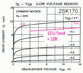
It's right there in the 2SK170 datasheet.
You are running very small bias so the current will be similar to the red line. This rises 1mA in 12V, which makes a 12K Source impedance.
But it curves. Using a smaller scale we find maybe 40K at high voltage and 4K at low voltage.
Your signal is very small, there is no point in running high voltage. So you are probably around 5K per JFET, 1.25K for the quad. +/-100% because you don't/won't know your actual operating point, and this is not a tightly controlled fabrication parameter.
That in shunt with your odd 2K resistor makes 0.77K, maybe 0.55K-1.1K.
For 1dB error at the 50Hz pole you need 10% accuracy of your "47K" resistor, 42K-52K. The ~~0.5K uncertainty of the JFET Drain is a 1% uncertainty of 50Hz corner, and pretty insignificant. 47K is a good value, though 25K or 100K would be fine also.
Attachments
Yes, it's supposed to be the modern European symbol for a resistor - but drawn with a general-purpose drawing program I don't know very well.
Many resistances and transistor types can work, for example 6.8 kohm and BC550CG.
No, the JFET's drain voltage is set by the voltage drop across the red LEDs minus the VBE of the extra transistor minus the voltage across the source resistor. This should result in about 6 V, probably just below 6 V. That's enough, because with cascoding there is almost no signal swing on the drains.
For optimal headroom, the remaining voltage has to be distributed evenly between the cascode transistor and the current source transistor. That boils down to a V??? of about 14.5 V.
Thank you very much, Marcel.
I will print out your instructions and refer to them for my next build - which will have a cascoding transistor.
I'll also add it to my LTspice circuit, to see what it does.
Andy
It's right there in the 2SK170 datasheet.
You are running very small bias so the current will be similar to the red line. This rises 1mA in 12V, which makes a 12K Source impedance.
But it curves. Using a smaller scale we find maybe 40K at high voltage and 4K at low voltage.
Your signal is very small, there is no point in running high voltage. So you are probably around 5K per JFET, 1.25K for the quad. +/-100% because you don't/won't know your actual operating point, and this is not a tightly controlled fabrication parameter.
That in shunt with your odd 2K resistor makes 0.77K, maybe 0.55K-1.1K.
For 1dB error at the 50Hz pole you need 10% accuracy of your "47K" resistor, 42K-52K. The ~~0.5K uncertainty of the JFET Drain is a 1% uncertainty of 50Hz corner, and pretty insignificant. 47K is a good value, though 25K or 100K would be fine also.
Brilliant - thanks, PRR!
Re. whether I should use 25K ... or 47K ... or 100K for the 'lead-in' res (R7), I get ~20dB loss across the passive RIAA network, so I was thinking of using 33K (in place of 47K) to decrease the signal loss?
Given the effective value of the gain res (R1) is actually much lower than 2K (when you take the Zout of the 1st gain stage into account) ... 33K gives an acceptable load.
Regards,
Andy
It's right there in the 2SK170 datasheet.
You are running very small bias so the current will be similar to the red line. This rises 1mA in 12V, which makes a 12K Source impedance.
But it curves. Using a smaller scale we find maybe 40K at high voltage and 4K at low voltage.
Your signal is very small, there is no point in running high voltage. So you are probably around 5K per JFET, 1.25K for the quad. +/-100% because you don't/won't know your actual operating point, and this is not a tightly controlled fabrication parameter.
Studying that diagram, PRR, I have a Qu.
In fact, my Drain current is down less than 5ma - so doesn't that mean I should draw your red line just above the 3rd graph from the bottom?
This is flatter - so only rising 0.5mV in 12v. Which makes a 24K Source impedance?
Adjusting your arithmetic, that suggests I should assume a 10K Zout per JFET, at my voltage - am I right? So 2.5K for the quad?
Andy
No. A passive RIAA network must have a midband loss of around 20dB. This is unavoidable. Have you done any reading on RIAA etc.? Have you ever thought about what the RIAA curve means and how to achieve it?andyr said:Re. whether I should use 25K ... or 47K ... or 100K for the 'lead-in' res (R7), I get ~20dB loss across the passive RIAA network, so I was thinking of using 33K (in place of 47K) to decrease the signal loss?
If you halve the input resistor, then all other resistor values in the network have to halve too, and all the cap values have to double.
No. A passive RIAA network must have a midband loss of around 20dB. This is unavoidable. Have you done any reading on RIAA etc.? Have you ever thought about what the RIAA curve means and how to achieve it?
Yes, I have read a lot about RIAA. I know the RIAA network I'm using atm has a ~20dB 1kHz loss but I hadn't twigged that this was absolutely unavoidable.
If you halve the input resistor, then all other resistor values in the network have to halve too, and all the cap values have to double.
Yes I know - but, from your post, I now understand that the new values will together produce the same dB loss!
So I'll keep the lead-in res at 47K.
Thanks,
Andy
If you look at the RIAA curve you will see that the mid-band is 20dB below the LF peak. That is why a passive RIAA network must give a mid-band attenuation of at least 20dB.
If you scale circuit impedances in a passive network by the same amount then the result is always the same gain or attenuation. This is because the network is essentially a frequency-dependent potential divider, and the loss for a potential divider only depends on ratios not absolute values. If you don't scale all impedances by the same amount then the network ceases to be an RIAA network but presents some other curve instead.
If you scale circuit impedances in a passive network by the same amount then the result is always the same gain or attenuation. This is because the network is essentially a frequency-dependent potential divider, and the loss for a potential divider only depends on ratios not absolute values. If you don't scale all impedances by the same amount then the network ceases to be an RIAA network but presents some other curve instead.
...the RIAA network I'm using atm has a ~20dB 1kHz loss...
And 40dB loss at 20KHz.
If your first stage gain is not >40dB, then the high frequency output after 1st stage and EQ is *lower* than the level you put in. Since your 2nd stage has at least as much noise as the first stage, the 2nd stage adds hiss.
This may be "tolerable" since a cartridge's response is very strong at high frequencies. But you can do better.
Much is unclear about what you want to do. Is this a MM preamp? (The 47K input makes me think so.) Then you probably do not need 4 devices parallel for 2SK170 from a 5K-50K source. If you must put in four devices, I do not know that Gate resistor is essential (depends on layout) but you probably need *four* Gate AND four Source resistors for equalizing current and suppression of push-pull VHF squirreliness.
I really do not understand 2KR1 R11 bleeding heavy DC current and lots of audio to ground, throwing-away gain which is usually precious in MM preamp work. Yes it does swamp uncertainty of EQ network impedances. Like I can "level" the upper floor of my house by parking a 2-ton truck on the high spots. There may be other ways.
You have five "adjustable" parts, more than most commercial designers can justify. (OK, a 5-tube radio has 7 trims, which was a significant cost, which is why ceramic filters and VCO tuners took over.) And some unlikely values (a 46r pot?). A 17n508 cap? Why not make everything adjustable and tune until happy (or terminally confused)?
Much is unclear about what you want to do. Is this a MM preamp? (The 47K input makes me think so.)
It's actually an MC phono stage. I use a 47K default res on the board because I build it with a pair of parallel input RCAs - so the effective value of the reses used in the load plugs (in parallel with 47K), comes out to be almost the same as the res value.
I use a much simpler circuit for MM which uses JFET pairs as gain stages.
Then you probably do not need 4 devices parallel for 2SK170 from a 5K-50K source. If you must put in four devices, I do not know that Gate resistor is essential (depends on layout) but you probably need *four* Gate AND four Source resistors for equalizing current and suppression of push-pull VHF squirreliness.
I use the 4 parallel JFETs to get the gain I need.
I'm interested in your comment that the Gate resistor is not necessarily needed. I had read that a Gate res on a JFET is required for stability?
If it really isn't needed (for stability) ... I'd rather get rid of it - as (as Joachim stated) it creates noise.
An individual source res for each JFET is something I'd like to avoid - and no HF problems have revealed themselves in listening. I do take care to match the quads to within 0.02ma Idss, though.
I really do not understand 2KR1 R11 bleeding heavy DC current and lots of audio to ground, throwing-away gain which is usually precious in MM preamp work.
The res in that position after each JFET quad, shunting to ground, is what influences the gain.
You have five "adjustable" parts, more than most commercial designers can justify.
Yes, it becomes a lengthy exercise to set it up correctly, when testing!
But 5 adjustable resistors are needed to be able to:
* set the Source current through each JFET quad to the desired level
* set the CCS resistor to give the desired voltage at the Drain of each gain stage, and
* adjust the final output - in particular, to exactly match R & L channels.
And some unlikely values (a 46r pot?). A 17n508 cap?
The required R & C values (as calculated by the passive composite RIAA network equations) are simply achieved by paralleling.
Andy
- Status
- This old topic is closed. If you want to reopen this topic, contact a moderator using the "Report Post" button.
- Home
- Source & Line
- Analogue Source
- Zin of the 2nd stage of a JFET-based phono stage when a pair of JFETs is used?