Hi,
I made my first phono stage a few months ago with a design based upon a TI app note. Thanks to help from people here I got that working and was pretty happy with the results. Since then I've been reading Small Signal Audio Design by Douglas Self (great, accessible book) and have realised that what I produced was far from optimal.
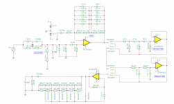
So here's my second attempt, it's a 35dB RIAA stage, followed by selectable high pass and low pass filters with a switchable gain stage at the output. The op amps are OPA1612, ceramics are C0G NP0 1% and resistors are thin film 0.1%. The electrolytics are Nichicon Muse bi-polar.
Because of the signal switching I've gone for a four layer PCB (first for me) with layers for signal (top), signal ground (2nd), DC ground (3rd) & power + switching (bottom). The relays will be controlled by a microcontroller off the board.
So any advice, comments or if you spot mistakes I'd be really grateful to know. It's Chinese new year at the moment so I'm hoping put my PCB order in at the end of February.
Thanks,
Simon.
I made my first phono stage a few months ago with a design based upon a TI app note. Thanks to help from people here I got that working and was pretty happy with the results. Since then I've been reading Small Signal Audio Design by Douglas Self (great, accessible book) and have realised that what I produced was far from optimal.
So here's my second attempt, it's a 35dB RIAA stage, followed by selectable high pass and low pass filters with a switchable gain stage at the output. The op amps are OPA1612, ceramics are C0G NP0 1% and resistors are thin film 0.1%. The electrolytics are Nichicon Muse bi-polar.
Because of the signal switching I've gone for a four layer PCB (first for me) with layers for signal (top), signal ground (2nd), DC ground (3rd) & power + switching (bottom). The relays will be controlled by a microcontroller off the board.
So any advice, comments or if you spot mistakes I'd be really grateful to know. It's Chinese new year at the moment so I'm hoping put my PCB order in at the end of February.
Thanks,
Simon.
Attachments
Thanks for spotting, I added the HPF and forgot to update the 47k to 150k.You have a 47K at the input, and then a 68K after the blocking cap. Load on the needle is 27.8K, an unconventional value.
Narrowest trace is 0.2mm, I can't find a spec for the minimum trace width on the PCB house website (pcbway.com), I'll ask the question when I submit the gerbers.Some of the pcb tracks are very thin.
They look on the limit to me of what the pcb house can do reliably.
I started off by looking at analogue switches mostly because of the cost and footprint benefits. But the specs for on resistance (and tolerance between channels), linearity and crosstalk gave me concerns - I'm sure a more experienced person would be able to pick the right component and design around the limitiations but I didn't have the confidence to do that.Have you considered analogue switches instead of relays ?
Thanks,
Simon.
Narrowest trace is 0.2mm, I can't find a spec for the minimum trace width on the PCB house website (pcbway.com), I'll ask the question when I submit the gerbers.
There are layout guidelines in the IPC-D-330 manual if you can find a copy on-line. A condensed version is available here: http://www.ceminc.net/Colonial%20DFM%20Guidelines%20Rev-C.pdf , page 23.
Personally, I do not go below 10mil track width (.254mm); below that, if the fab over etches the copper, the reliability can suffer (broken traces).
PCBWay.com charge 55 USD for 10pcs 100x100mm plus shipping. The price jumps to >100 USD if one of the dimensions is greater than 100mm so I need to trim 2mm off the length before I order.
I found the specs for track width and I think they'll charge no extra as long as the tracks are >6mil.
I've used them loads of times and the last few orders have arrived 7 days after submitting the gerbers. Very reliable and good quality.
I found the specs for track width and I think they'll charge no extra as long as the tracks are >6mil.
I've used them loads of times and the last few orders have arrived 7 days after submitting the gerbers. Very reliable and good quality.
PCBWay.com charge 55 USD for 10pcs 100x100mm plus shipping. The price jumps to >100 USD if one of the dimensions is greater than 100mm so I need to trim 2mm off the length before I order.
I found the specs for track width and I think they'll charge no extra as long as the tracks are >6mil.
I've used them loads of times and the last few orders have arrived 7 days after submitting the gerbers. Very reliable and good quality.
Plus import duty.
The last order I got they charged £21 for import duty.
It looks as if you are using Eagle layout software?
Looking at the ground plane, you can avoid the large voids by enabling orphans in the ground pour set up (select the info tool and click on one of the polygon edges to see its properties). This can improve consistency as the large areas of copper take longer to etch than if there are just small gaps between ground pours and signal traces.
It also appears that the spacing between ground pour and signals is quite small, possibly smaller than the .2mm signal width. In the same ground pour properties, verify that you have a non-zero value for isolate, other wise it will default to 8 mils and may create shorts with signal traces. I usually spec 10 mils for low voltage circuits, 20-25mils for HV.
Using the specs in the on-line link I provided, you can populate the DRC fields (under the tools menu). Running the DRC will then show any violations and allow you to correct them before spinning a board.
Overall the board looks very good. The silk screen in some of your library parts (1206 Resistors/Caps?) are overlaid onto the pads. Most fabs will automatically clip the silk screen to prevent this, but if they don't, it can make soldering problematic. Always best to prevent this in the first place if you can by modifying the library part.
If you don't already have a Gerber editor tool, I would suggest looking at ViewMate Deluxe from Pentalogix. Single user license is ~$95. The editor will allow you to make changes that are not possible in the PCB layout software and can really clean up a load of sins with it.
Last edited:
It seems very complicated and I am having trouble following the design, what are all of these relays for?
Depending on the op-amp used you probably don't really need the input capacitor.
Have you considered headers with jumpers for things that don't need to be changed in regular use.
I would go with 15 - 20 mil traces and avoid the issues inherent in pushing their process that close to the limit, 7.87 mils is pretty narrow. Small registration errors become rather significant with such small geometry.
At work we only use such small traces with devices using very fine pitch or ball grid.
I've designed well over a dozen phono stages completely from scratch and when I look at your design I'm lost. Simpler devices tend to be more reliable and easier to get working properly all things being equal.
Thanks both for taking a look at the designs.
Pyramid, yes I am using Eagle - thanks for the pointers, I'll follow your advice and update the design rules. I'd not considered using a gerber editor, I'll take a look at that too.
Kevinkr - I think I've made the design look more complicated than it is, I need to work on my schematic drawing skills. I think part of the problem is the way I've constrained myself with the dual op amp package and dpdt relays - that left me with traces all over the place and needing to put both channels on one board. Perhaps the linked picture of the TinaTI schematic that I started with is a better representation of what I'm trying to do.
The relays are there to switch the filter stages in and out and adjust the gain (I'm thinking I could maybe make do with fewer gain steps). Jumpers would make the layout simpler but I'd like to be able to change these settings without opening up the chassis. I used dip switches next to the RCAs in a previous design but the routing for those wan't much simpler.
The track widths are a concern I'm going to see if I can do something about those. I do have a question though - would errors introduced by using too small a track width be there from the start or could they emerge over time i.e. the amp would stop working at some undefined point in the future?
Thanks again for taking the time to look at the designs.
Simon.
Attachments
Thank you for posting the Tina Ti schematic, it is much clearer, and I now understand what is going on.
I would probably avoid using the dual op-amp symbol in the future, and use one that treats them as separate parts (U?A/U?B) this will allow you to create a schematic with a logical signal flow.
The problem with very small traces is two fold, you could have an immediate issue, and over the longer term if there is any etchant left smaller geometry features are much more vulnerable to damage. I have a friend who swears by pcbway, and I use pcbcart. The smallest trace width I usually use is 15 mils.
1) The Riaa Caps are both wrong.
Left side should be 27n6 instead of 26n6, right side should be 7n8 instead of 6n8.
2) C3, 300p should be much lower. The capacitance of the phono cable will already be at least 150pF.
3) I don't understand the variable gain setting around U4. This doesn't work and should be corrected.
4) in this last diagram you have the OPA1612, a dual op amp which is not suitable for an MM. But in the earlier diagram you have the OPA1652, a quad fet op amp. That is a good choice.
Hans
Hi Hans, that was an old schematic that I used to simulate the circuit before creating the Eagle schematic and layout (I thought it would be simpler to read than the horrible one I put up before), but it is pretty much what I implemented.
1) The RIAA values are the ones you suggest (27n6 & 7n8) perhaps the top two 1n caps got cut off in your view of the schematic?
2) I didn't think of taking into account the capacitance of the cable - thanks for the advice.
3) I've simulated the gain setting in TinaTI and it works as expected... I'd be interested to know why you don't think it will work in practice.
4) Agreed
Thanks for your comments.
Simon.
1) On my iPad the 1nF caps were not visible indeed.Hi Hans, that was an old schematic that I used to simulate the circuit before creating the Eagle schematic and layout (I thought it would be simpler to read than the horrible one I put up before), but it is pretty much what I implemented.
1) The RIAA values are the ones you suggest (27n6 & 7n8) perhaps the top two 1n caps got cut off in your view of the schematic?
2) I didn't think of taking into account the capacitance of the cable - thanks for the advice.
3) I've simulated the gain setting in TinaTI and it works as expected... I'd be interested to know why you don't think it will work in practice.
4) Agreed
Thanks for your comments.
Simon.
Question, why do you use so many caps, 10 in total, instead of 22n+5n6 and 6n8+1n, that will save you a lot of PCB space.
3) Why did you insert C13, 1000uF ? This cap will cause plops when switching and should be removed.
5) When using 1Meg for R3, you could replace C4 by a much better "normal" 100nF cap instead of a 22uF electrolytic. The OPA1652 has an Input Impedance of 100Meg.
Hans
I specced all the caps and resistors based upon what I can get from RS Components, they don't stock the cap values you suggest in C0G/NP0 1%. I've just checked and I can get those values from Farnell - so I think I'll follow your suggestion and save a bit of money.
3) I must admit that C13 is the one component that I don't fully understand, I've included it because Douglas Self uses one in his switchable gain stage. I believe it is for DC blocking and R24 provides the feedback for DC to prevent popping. I'm planning on testing with and without the cap to see if I can get a better understanding of what its effect is.
5) From what I've read as long as C4 has negligible voltage across it within the audio band and low current it should not have a noticeable contribution to distortion. Do you think a polyester cap would be better in this application?
I've been working on a new layout based upon the feedback I've got here, I've still to get the labelling readable but I've included the PDFs below.
Thanks,
Simon.
Attachments
R24 is important, because when switching there is a moment that relays are moving from one position to the other.3) I must admit that C13 is the one component that I don't fully understand, I've included it because Douglas Self uses one in his switchable gain stage. I believe it is for DC blocking and R24 provides the feedback for DC to prevent popping. I'm planning on testing with and without the cap to see if I can get a better understanding of what its effect is.
5) From what I've read as long as C4 has negligible voltage across it within the audio band and low current it should not have a noticeable contribution to distortion. Do you think a polyester cap would be better in this application?
I've been working on a new layout based upon the feedback I've got here, I've still to get the labelling readable but I've included the PDFs below.
Thanks,
Simon.
Without R24, gain would be infinite and would cause a giant glitch in the output voltage until the Relay has settled.
C13 on the other hand is not blocking anything, and should not be used.
C4 will have little or no voltage to bridge, this means that you could just as well take it out.
But in case you want a cap at that place, it better not be an electrolytic cap, despite all positive distortion figures.
A polyester cap will be definitely better, but no cap at all would have my preference.
Hans
- Status
- This old topic is closed. If you want to reopen this topic, contact a moderator using the "Report Post" button.
- Home
- Source & Line
- Analogue Source
- Phono Stage PCB Layout