I've been working on a new layout based upon the feedback I've got here, I've still to get the labelling readable but I've included the PDFs below.
Thanks,
Simon.
The track width looks better, but the ground pour is still very tight.
Also, some of the tracks are very close to the corners of pads (resistors adjacent to U2). The tracks that make contact with U2 should enter and leave the pads in-line with the long dimension of the pad, there is no reason (and no room) to exit on the side of the pad and make a 45° turn. If you run the DRC it should highlight any of these violations. You can save and load different DRC profiles if you like, or set up preferred parameters and save as the default profile.
I share the same concerns as Pyramid.
You have so many options with a 4 layer PCB that there is no reason at all to have traces so close together and so close to pads and vias.
Be also aware that there is a large capacitive coupling between traces that are adjacent over a longer distance when positioned so close together.
Another point that puzzles me:
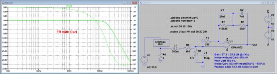
With a Cart connected, FR is at ca. -30dB at 100Khz, see below.
Yet you have also added a supersonic filter which has its -3dB at 100Khz.
This doesn't seem to add anything at all ?
Hans
You have so many options with a 4 layer PCB that there is no reason at all to have traces so close together and so close to pads and vias.
Be also aware that there is a large capacitive coupling between traces that are adjacent over a longer distance when positioned so close together.
Another point that puzzles me:
With a Cart connected, FR is at ca. -30dB at 100Khz, see below.
Yet you have also added a supersonic filter which has its -3dB at 100Khz.
This doesn't seem to add anything at all ?
Hans
Attachments
By 'tight' do you mean that there's not enough clearance? I increased that in the design rules to 8mil - perhaps 10 would be better.The track width looks better, but the ground pour is still very tight.
I hadn't noticed that the tracks exit the pads in that way - seems to be the default way that eagle routes them. I can't find anything in the design rules related to that so I'll go through and do it by hand.Also, some of the tracks are very close to the corners of pads (resistors adjacent to U2). The tracks that make contact with U2 should enter and leave the pads in-line with the long dimension of the pad, there is no reason (and no room) to exit on the side of the pad and make a 45° turn. If you run the DRC it should highlight any of these violations. You can save and load different DRC profiles if you like, or set up preferred parameters and save as the default profile.
My reasoning for running the traces in parallel was to keep the pours as intact as possible. The parallel traces are to and from the relays which will only be operated one at a time. Do you think this will cause a problem in practice?Be also aware that there is a large capacitive coupling between traces that are adjacent over a longer distance when positioned so close together.Hans
You're right, I didn't include the cart in my model... which seems stupid in retrospect but I didn't think of it. As you can see with my original model the response starts to rise at 100kHz and that's why I included the filter.Another point that puzzles me:
With a Cart connected, FR is at ca. -30dB at 100Khz, see below.
Yet you have also added a supersonic filter which has its -3dB at 100Khz.
This doesn't seem to add anything at all ?
Hans
Now I've included the cart I'm also a bit bothered about being 3dB down at 20k.
I think you're right I can drop it.
Attachments
By 'tight' do you mean that there's not enough clearance? I increased that in the design rules to 8mil - perhaps 10 would be better.
Yes, I think the gap is too small between tracks and ground plane. Setting it to 8 mil in the DRC will only notify you of errors when you run the DRC tool. The gap is actually set in the properties for the polygon. Select the info tool and left click on any of a polygon's sides to bring up the properties for that polygon. The 'isolate' parameter determines the gap. If it is set to zero, the program will default to ~8mil. I usually set it to 10-12mil for low voltage designs, 20-25mil for HV. You can also use Change\Isolate tool; select the gap width from the menu then left click on one of the polygon sides to change it.
I hadn't noticed that the tracks exit the pads in that way - seems to be the default way that eagle routes them. I can't find anything in the design rules related to that so I'll go through and do it by hand.
I wasn't aware you were using the auto-route capabilities. I seldom use that unless I'm doing a large digital PCB with lots of address/data busses, as it seems to manage those better than I can do manually. On a PCB with the complexity of yours, I would use manual routing, but that's my personal preference.
Not sure why it would choose to lay down tracks like that; again, I'm not as familiar with the autorouter. It might use the DRC settings, and if set too low (or not specified), would not see a clearance problem by exiting between the pads.
Last edited:
It's not auto-route, it's just when I drag a trace out of a pin it lays it down that way... I just need to anchor it at 90 degrees rather than let eagle do it's thing.
OK, it's easy to change that. When you have the route tool selected and left click on an air-wire to start routing, you can change the direction of exit/entry and the type of track (orthogonal, 45 deg, arcs, any angle) by repeatedly right clicking the mouse button. It's not uncommon to select a type, create several segment endpoints along the way, then change to a different type as you move around parts and terminate at the next pin. You can do this on-the-fly as you are laying down the track; no need to stop and change the track type, just right click the mouse.
You can use the ripup tool to undo segments (turn them back into air-wires) that you do not like, but if you double click or click too fast, it will ripup the entire net (track). F9 (undo) is your best friend.
Just another suggestion.
As you may have noticed, I prefer to have as little caps in the audio path as possible, especially avoiding electrolytic caps.
Distortion figures may look very promising in certain situations, but according to my experience, less is more.
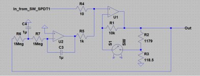
Since that you now have decided not to add the ultrasonic filter, you could use this Op Amp U2 as a servo to keep the output voltage below 0.5 mV, low enough to also be able to remove C12, and R25.
The OPA1652 has an Vos of 0.5 mV, so this op-amp can be very wel used for the purpose, see diagram below.
What you have at the input of U4 without servo , is the combined offset of U1, U3 and U4.
When steering U4 with this servo, DC output voltage will be reduced to 0.5 mV, the questionable need for having C13, the huge 1000u in the audio path, is then also completely gone.
Without C4, the preamp will have an almost cap free audio path..
Hans
As you may have noticed, I prefer to have as little caps in the audio path as possible, especially avoiding electrolytic caps.
Distortion figures may look very promising in certain situations, but according to my experience, less is more.
Since that you now have decided not to add the ultrasonic filter, you could use this Op Amp U2 as a servo to keep the output voltage below 0.5 mV, low enough to also be able to remove C12, and R25.
The OPA1652 has an Vos of 0.5 mV, so this op-amp can be very wel used for the purpose, see diagram below.
What you have at the input of U4 without servo , is the combined offset of U1, U3 and U4.
When steering U4 with this servo, DC output voltage will be reduced to 0.5 mV, the questionable need for having C13, the huge 1000u in the audio path, is then also completely gone.
Without C4, the preamp will have an almost cap free audio path..
Hans
Attachments
Last edited:
Thanks, that's a good idea, although I've had mixed success with implementing servos in the past - this will be another area to read up on.
I'm not familiar with the servo design that you've presented but I think I understand it... any DC present at the output of U1 will drive U2 to output the inverse voltage cancelling out the DC at the non-inverting input of U1? I'm trying to understand the purpose of C3, is it for stability or to prevent amplification of AC from the grounded input? If you know what I mean... as I'm sure you can tell this is still a learning exercise for me.
I'm not familiar with the servo design that you've presented but I think I understand it... any DC present at the output of U1 will drive U2 to output the inverse voltage cancelling out the DC at the non-inverting input of U1? I'm trying to understand the purpose of C3, is it for stability or to prevent amplification of AC from the grounded input? If you know what I mean... as I'm sure you can tell this is still a learning exercise for me.
R6 + C3 and R7 + C4 in combination with U2 are the two low pass filters forming the servo.Thanks, that's a good idea, although I've had mixed success with implementing servos in the past - this will be another area to read up on.
I'm not familiar with the servo design that you've presented but I think I understand it... any DC present at the output of U1 will drive U2 to output the inverse voltage cancelling out the DC at the non-inverting input of U1? I'm trying to understand the purpose of C3, is it for stability or to prevent amplification of AC from the grounded input? If you know what I mean... as I'm sure you can tell this is still a learning exercise for me.
And you are right, any DC at the output of the preamp, no matter what the source is, will be reduced to Vos of the Servo, in this case 0.5 mV.
Hans
I'm going to update the design to include the servo. One thing that's bothered me in the past is whether servo failure is any more likely than a blocking cap failing short circuit (which I'm assuming is very unlikely). I've have some recollection of seeing a servo protection circuit being used in other applications. I've got dc blocking on the input to my power amp so I guess it wouldn't be disastrous for me but I'm just curious.
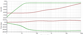
Having now included the cart in the TinaTI model I've also realised the impact of the input load capacitance on the 10-20kHz response of the amp. I think I'll make this adjustable, probably just a small range of values but by dip switch rather than relay. Is the -3dB at 20kHz a generally accepted artefact of the cart or is there something that can be done to eliminate it?
Having now included the cart in the TinaTI model I've also realised the impact of the input load capacitance on the 10-20kHz response of the amp. I think I'll make this adjustable, probably just a small range of values but by dip switch rather than relay. Is the -3dB at 20kHz a generally accepted artefact of the cart or is there something that can be done to eliminate it?
I have never ever encountered a servo failure. With a high quality PCB and reliable components, there is no risk at all.I'm going to update the design to include the servo. One thing that's bothered me in the past is whether servo failure is any more likely than a blocking cap failing short circuit (which I'm assuming is very unlikely). I've have some recollection of seeing a servo protection circuit being used in other applications. I've got dc blocking on the input to my power amp so I guess it wouldn't be disastrous for me but I'm just curious.
Having now included the cart in the TinaTI model I've also realised the impact of the input load capacitance on the 10-20kHz response of the amp. I think I'll make this adjustable, probably just a small range of values but by dip switch rather than relay. Is the -3dB at 20kHz a generally accepted artefact of the cart or is there something that can be done to eliminate it?
You are right that the load capacitance has a substantial impact on FR.
But the Cart manufacturer knows very well what to do to prevent the dip at 20 Khz, so don't get blinded by simulations.
Although these sims give a reasonable idea, the real thing is always different and yes, the proper capacitance will be required to get the best possible transfer.
There is an alternative to this by feeding the Cart output signal to the virtual input of an Op Amp.
By doing that, capacitance plays no longer a role at all, but fine tuning becomes even more important and differs quite a bit from Cart to Cart, making this solution less universal.
Hans
To keep noise low in the signal path, I used 100 Ohm for R4.Hans - I'm just re-working the design and I was wondering how you came up with the values for R4 & R5 in post 28?
Thanks,
Simon.
For very low frequencies where the servo is active, the ratio of R5/R4 is determining the amplitude of the signal coming from the servo.
When a 1 Volt 1 Hz signal is entering R4, the servo will try to cancel this with a signal of opposite polarity, in this case having an amplitude of 10 Volt.
Making R5 larger will lead to clipping of the servo thus generating large amounts of distortion.
So I used just a large safety margin.
Changing R5 also has effect on the two caps C3 and C4.
When making R5 larger, C3 and C4 should become smaller in the same ratio.
Making R5 10K, results in C3 and C4 of 10 nF, but the overload margin will be decreased by a factor 10 at the same time.
But you could change R4 and R5 to 1K/10K without any effect. Noise will still be low.
Hans
Thanks everyone for the help so far. I tried to incorporate all of the advice, so I went back and re-drew the schematic (slightly but not altogether better). I can't find a way of creating a double op-amp package that allows me to split out the individual op amps in the schematic view.
I've also re-created the layouts with updated design rules. All the tracks are now 20mil / 0.5mm.
I've checked and double checked but I'm sure there are still mistakes in there, I'll go over the whole lot again before hitting the order button.
Does this look like an improvement?
I've also re-created the layouts with updated design rules. All the tracks are now 20mil / 0.5mm.
I've checked and double checked but I'm sure there are still mistakes in there, I'll go over the whole lot again before hitting the order button.
Does this look like an improvement?
Attachments
At a first glance it looks much better, although reading your circuit diagram is like trying to solve a multidimensional Sudoku.
The PCB looks much better too.
is it possible to remove all isolated pieces of copper, they are acting as antennas and have no further function.
One other question, 45 degrees turns are much better than at 90 degrees, so you did that well, but isn't your layout program able to turn those into nice arcs at a later stage ?
And to check possible violations of rules, doesn't your software have a provision for that, because it is almost impossible to find all violations with the naked eye.
Sorry for asking so many questions.
Hans
Ha... yes you're right - it gives me a headache when I look at it.At a first glance it looks much better, although reading your circuit diagram is like trying to solve a multidimensional Sudoku.
I can... I was following Pyramid's advice from post #11. I use Eagle software and it seems to be all or nothing with the orphan sections of a pour. I was also a bit worried about the boards warping as a result of some of the larger voids.is it possible to remove all isolated pieces of copper, they are acting as antennas and have no further function.
I can do arcs with Eagle... I may have a play and see how I get on.One other question, 45 degrees turns are much better than at 90 degrees, so you did that well, but isn't your layout program able to turn those into nice arcs at a later stage ?
I've run a DRC, so I know the layouts align with the design rules and schematic, I really need to double check the values in the schematic and make sure the circuit matches the one I simulated.And to check possible violations of rules, doesn't your software have a provision for that, because it is almost impossible to find all violations with the naked eye.
Thanks for your help, I really appreciate it.
I knew I'd mess up somewhere with this... I double checked the schematic against the simulation in TinaTI and hit the order button with pcbway. Then when ordering the components realised I'd specced 1uF 0805 SMDs in the sub-sonic filter  . As far as I can tell these don't exist as C0G NP0 types so I'm trying to work out an alternative.
I'm resigned to the fact I need to correct the design for a permanent solution but in the mean time is there a capacitor (even a leaded type) that I could use to test? Ideally lowest thd and minimum tolerance in that order of importance.
Any ideas would be great.
. As far as I can tell these don't exist as C0G NP0 types so I'm trying to work out an alternative.I'm resigned to the fact I need to correct the design for a permanent solution but in the mean time is there a capacitor (even a leaded type) that I could use to test? Ideally lowest thd and minimum tolerance in that order of importance.
Any ideas would be great.
- Status
- This old topic is closed. If you want to reopen this topic, contact a moderator using the "Report Post" button.
- Home
- Source & Line
- Analogue Source
- Phono Stage PCB Layout