In general this topologies are used for balanced input mode:
http://www.ti.com/ods/images/SBOS247C/first_page_sbos247.gif
http://www.ti.com/lit/ds/symlink/ina217.pdf
http://www.tubecad.com/2013/01/26/Good OpAmp Circlotron.png
but the circuit below show a version with basically only a single operational amplifier (new for me).
What are here the pros and cons ?
Are there papers with general description concerning this approach ?
Thank you for your advices.
P.S.
this topology allows additional two unbal. input modes for moving coil cartridges:
1) one mode with high impedance input (non inverted input, called "MD input")
for this mode an additional input resistor with arround 100 ohms or less is necessary (integrated in the connector plug for the unused input socket)
The switchable resistor bank serves only for the voltage gain factor.
2) one mode with low impedance input (inverted input), called MC input (Binder input socket "711" series - high impedance PIN unused, i. e. N.C.)
for this mode the switchable resistor bank serves for the suited input impedance and the voltage gain factor at the same time.
This is good to understand.
Attachments
Last edited:
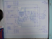
This I want to know.This circuit has plain unbalanced input and output. Nothing in common with AD846 and the other topologies you linked.
Where was it published?
The weakness is the capacitors between the base of T1-T2, they spoil the sound.
The circuit is from the OMTEC Phono RIAA preamp model CP-1 (1994) - go to
Omtec Antares CP1-i/CP-1i - Testreview in English and Schematic wanted
The used transistors are 2SB737 and 2SD768
Last edited:
This I want to know.
The circuit is from the OMTEC Phono RIAA preamp model CP-1 (1994) - go to
Omtec Antares CP1-i/CP-1i - Testreview in English and Schematic wanted
The used transistors are 2SB737 and 2SD768
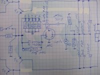
The transistors have very low Rbb and are a good fit for such a virtual ground application.
You sometimes see this in DAC discrete I/V stages - the concept and the issues are the same.
The AD846 is obsolete but a similar device with less Iout capability is still available, the AD844.
Jan
Some years ago, i played with an ad844 and similar discrete incarnations. With discrete, i did not manage to get low enough input offset, and offset drifting as well.
You might find some q's from that-corporation that can replace the obsolete 2sb737
In some of the huge joachim-gerhard-phono-threads one can find something similar, i think.
You might find some q's from that-corporation that can replace the obsolete 2sb737
In some of the huge joachim-gerhard-phono-threads one can find something similar, i think.
- Status
- This old topic is closed. If you want to reopen this topic, contact a moderator using the "Report Post" button.