Quite right Joachim little blob of solder between the pins of one Jfet either the one I mentioned or the the ones at the left most of the boards on the R2 version which had the different foot print now improved on the R3.
In the mean time I got little disaster in my hands as I have managed to mess up the second channel I was working on and now it has really nasty hiss.
In the mean time I got little disaster in my hands as I have managed to mess up the second channel I was working on and now it has really nasty hiss.
Ricardo had a problem with the buffer that did the output on many volts.
I think it was a short on the PCB.
I have just double checked on both boards every single solder joint and found not a bit no short and all parts at the proper place.
What can I do next up. Alfred have you an idea.
Werner
have you put the "Neumann" resistor or a wire? You cannot leave that space open.....
Neumann resistor 220 ohm
Hi Werner, can you confirm that the input voltage (measured at the input pins) is +2.5V, and the output voltage is +15V? How about VCASCH and VCASCL, and the voltages across the 6800uF caps?
Good morning lads
Hi Alfred, I have just measured (Fluke 787 from our lovely electricians)
UPLUS = -18,13
UMINUS= +18,13
INPUT = +2,48
OUTPUT= +15,23
VCASCH= +14,49
VCASCL= -14,56
Across the 6800 uF caps plus side +1,73
Across the 6800 uF caps minus side -3.16
EXI RIAA= +15,23
Nearly the result
Maybe interesting as well, with the amp plugged the heat sink temperatur
is down (from 50 without amp) to 38 degree after 30min
Have a nice one
Werner
That is normal, if the amp is not connected then the PSU dissipates all, with the RIAA connected then dissipates about halve of the energy.
Hi Werner
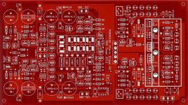
Please see the attached pic of the board where I included parts numbers.
The output buffer fets 90 and 99 are in the center of the board.
Once I had to replace 99 to get things working.... also the top fet 90 (J310) should be chosen with a high Idss / Vp otherwise the buffer might not work properly and produce big offset.
Attachments
Tanks for posting that Riccardo loads of work there.
I am back on after the Toshiba transplant and delighting neighbors with same nice tunes.
First impression is more focus and solid sound stage.
I have not done the Jfet change 6.4 C in the loft and 4 in of snow outside lovellly.
Just in case remember that pin out for J fet change...
I am pretty sure that there is much more to be had out of this baby and I am a bit reluctant to start with the R3 boards till we know a bit more about any progress with the German Forums.
What up boys?
First impression is more focus and solid sound stage.
In my limited experience, the biggest improvement as far as sound stage perception goes is derived from proper grounding techniques and especially taking ground return currents into account. Sadly, this will probably require a new pcb. R4?
That is normal, if the amp is not connected then the PSU dissipates all, with the RIAA connected then dissipates about halve of the energy.
Thanks Frans, now I am 100% sure that the PSU,s are working
In my limited experience, the biggest improvement as far as sound stage perception goes is derived from proper grounding techniques and especially taking ground return currents into account. Sadly, this will probably require a new pcb. R4?
I second that
") (improvement wise).
(improvement wise).Hi Werner
Please see the attached pic of the board where I included parts numbers.
The output buffer fets 90 and 99 are in the center of the board.
Once I had to replace 99 to get things working.... also the top fet 90 (J310) should be chosen with a high Idss / Vp otherwise the buffer might not work properly and produce big offset.
Thanks Ricardo that picture is very helpfull for me.
I will change 99 and 90 straight away. Can you or someboby else
tell me how I can measure Idss and how I can check 2SK 170 or J 107
I have no clue,
Take care
Werner
New R4 PCB needed well maybe, but noting wrong with one I got, provided one does proper grounding to start with and somebody that heard my Paradise R2 can vouch for proper execution of that.
So if you got boards for R3 don't despair Hesener did pretty good job IMO
I really doubt that I could do better especially as there is much more than grounding involved
So let's not water the wine please I am Just reporting on one change that can be easily done.
Wow can't you tell me giving up smokes...
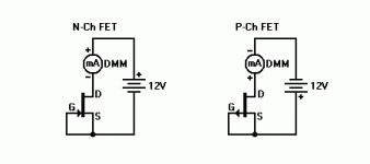
Hi Werner you can test the IDss I think is called sum think like that as in picture
Place 100 Hom's resistor where the Ammeter is and you can measure the V drop
I am making a rig to test evveritink but that is work in progress Got diverted...
as gate and source are connected only the self biasing current go trough the resistor
for 2SK170 BL you should get between 7 and 10 ma depending on the J fet.
I am going to post picture of work I did on that so far here
http://www.diyaudio.com/forums/swap-meet/226166-paradise-bcxxx-40-a.html#post3418819
Attachments
Last edited:
- Home
- Source & Line
- Analogue Source
- Paradise Builders