This reminds me that at some stage, much earlier in this thread i had some problems with the choice of Q90/Q99. There simply wasn't sufficient voltage across Q99 and i had to find a suitable Q90. Not sure if this was just a freak occurrence, as apparently my build is ultraprone to those, or some advice towards the selection of the fets can also be incorporated in the build guide.
Eventually it turned out that both channels' output buffers were also running at very different currents and for the sake of obtaining better symmetry had to replace R15 with a multiturn pot.
Cool request.
Inittialy I had issues with the output buffer also.... solved them by replacing the fets but did not understand the reason.
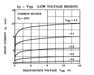
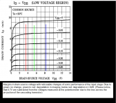
The top transistor in the Fet cascode has a certain voltage between gate and source, the so called Ugs or Vgs. The transistor down in the cascode, say the 2SK170BL runs at near zero Ugs. The difference in Vgs of the top transistor and the main transistor is the voltage that develops over Drain-Source of the down ( main Fet ) transistor. That voltage should not be too low because the down transistor is not very linear at very low voltages. Also ideally the Vgs diffenence should be the same in both channels. That requires to select the top transistors for Vgs, similar and as high as possible. Something between 3 and 5V is what we usually aim for.
You can interpolate the linearity of the 2SK170 from this curve that shows idle current at several voltages. You see that the first 2V are strongly bend. We would like to avoid that region. Over 3 V the curve is nearly straight. That means that the J-Fet is a very good constant current source in that region and that transfers into good linearity as a buffer.
This is of cause without cascoding and without the cascode current source we have in the Paradise. this two measures plus choosing the right condition for idle and Vgs give the Paradise buffer its exceptional linearity as long as the buffer works in class A.
This is the case when no more then the idle is drawn. For example we have 8mA idle and a 10kOhm load. The buffer can swing 80V in class A into that load. That is of cause not possible because we run the buffer on only plus-minus 18V.
Attachments
Last edited:
I grew used to set Vds between 8 and 12v for the k170... more will only increase dissipation IMO.
When you say we must choose J 310 by Vgs.... How ?
I know there is linearity between Vp and Idss in the same batch of fets http://www.diyaudio.com/forums/parts/227889-2sk170bl-vp.html#post3328098
So maybe we ca choose the J310 by Vp (matching them at higher than 5v for example)...
When you say we must choose J 310 by Vgs.... How ?
I know there is linearity between Vp and Idss in the same batch of fets http://www.diyaudio.com/forums/parts/227889-2sk170bl-vp.html#post3328098
So maybe we ca choose the J310 by Vp (matching them at higher than 5v for example)...
Well, in the La Boheme phono this is for the input stage working in transconductance mode . When you do the Vds voltage too high in an input of a phono stage the noise will go up because of rising gate current so it is a compromise between linearity and noise.
For the paradise buffer 3 to 5 V is fine.
For selecting Vgs in the J310 cascode Fet you can simply build the paradise buffer with Idss selected 2SK170. You can build a little jig from DIL8 sokets where you can insert the J310 and then simply measure in the real circuit.
For the paradise buffer 3 to 5 V is fine.
For selecting Vgs in the J310 cascode Fet you can simply build the paradise buffer with Idss selected 2SK170. You can build a little jig from DIL8 sokets where you can insert the J310 and then simply measure in the real circuit.
Last edited:
Sorry guys for disturbe.
I reed every single word of this thread an do like all of you but now I ran into trouble.
I solder the PCB´s with all the hints and tricks you gave me, matched the NPN and PNP in a little higher range (12%) and now this:
I managed to rise the powersupply with 24,7V put it in the powerinput and trimm the V+ and V- to +-18,00 V. After a Test of 8 hours I retrimm from 17,92 to 18,00V again. After that I solder the bridge and let the Caps settle in.
And here is the problem. after 8 hours settling I have the problem, that 2 Caps (V- 6800/6,3V) are wet on top and give little blisters. With other words they are gone.
What made I wrong? Hope for help
Thanks Christian
And here is the problem. after 8 hours settling I have the problem, that 2 Caps (V- 6800/6,3V) are wet on top and give little blisters. With other words they are gone.
What made I wrong? Hope for help
Thanks Christian
Wrong polarity on the caps.
Replace those by new ones in the correct position.

Thank you Alfred for your comprehensive explanation and i understand only some of it due to my limited knowledge. To clarify a few things: so if i change the input loading to 20K it should make no difference to the voltage at pin6 of IC then just leave it alone? and if it rises then may have to change the input transistors due to leakage current of BC junction?Hi,
the test points all have a square layout and are labelled, except the test points right next to the emitter resistors of the current sources. The test point you are referring to might be round, in which case I think it is a "via" (connection between top and bottom layer of the PCB). Yes, that may be the output connection of the servo (== pin 6 of the opamp), this line is pretty long and winding....
The servo giving such a large voltage means it has to compensate a certain offset of the input stage. Remember the servo's impact is pretty weak, and deliberately so, so that voltage can reach several volts both ways. It should stay within +/-12 V though, in order to not leave the linear output range of that opamp. 5V is therefore OK. Best would be 0V, but that only happens with perfectly matched input stage, current mirrors, and output buffer with no offset.
While the mirrors's design is very clever so their impact on offset is negligible, the other two sources of offset may be the cause. On the output buffer, if the JFET Q99 has a high IDSS, the voltage on its gate will have to be negative so it operates at the current dictated by Q91+R15. So in order to have zero output offset, the voltage at its gate will have to be negative, so the servo must steer it that way. In my case, the voltage there is -1.5V (as documented in the annotated schematic in the assembly guide). Now, you could run the output buffer at higher current, by reducing R15, and thereby reducing this offset, but thats not needed for performance or sound.
On the input stage, if the current gains are not matched well enough between the NPNs and the PNPs, you may see that type of offset as well. In fact, it should be different for different values of input load resistance (you would probably have to look at values of 10K or higher to see something). It may also be that there is one transistor that exhibits base-collector leakage current, this is VERY rare but sometimes individual transistors excape the test program at manufacturing. You may want to try input resistors of 10K and 20K just to see if the offset changes. If it doesnt than just live with it, you should be fine. If it does, you may want to check if you can come up with another set of input stage transistors.
I would also suggest you remove that 10 Ohm resistor in the ground wire. The ground connection from the star ground to the ground connection on the PCB should be as low-ohmic as possible. Rather put the 10 Ohm in the ground connection of the power supply. In fact, the assembly guide has a detailed schematic from Frans on how to do the grounding on the power supply side which is very good. You want to have the TT ground, the phono preamp case ground and the PCB grounds as closely linked as possible. Please do connect the output RCAs to the same star ground. The power supply wiring on your picture is good.
hope that helps.....
Quan
I have no pet, so no cat at all
unfortunately I have no photo of my boards, but if I look at them (sink on the right hand side) all of the white stripes (locat minus of the caps) look straight up.
Other suggestions?
Did you make any measurements on the boards just after power on ?
No, just V+,V- and the power in (+24,7V and -24,3V)
See PradiseBuilders #155 Vdc input voltage minimum simulated. it would be nice to have about a volt more, but it will work
(The linked message states that 24V is marginal). (Do I have to post this twice )
Last edited:
Thank you Alfred for your comprehensive explanation and i understand only some of it due to my limited knowledge. To clarify a few things: so if i change the input loading to 20K it should make no difference to the voltage at pin6 of IC then just leave it alone? and if it rises then may have to change the input transistors due to leakage current of BC junction?
Quan
yes exactly
Hello Alfred,
I second Benedetto's request ....
"Hello Alfred,
is it possible to you to put the link to your
fine, constantly actualized Builders Guide in your underline ?"
pleeeeeeaaaazzzzzz ;-)
It will make things much easier, you would even get less support questions...
JBdV
will figure it out
No, just V+,V- and the power in (+24,7V and -24,3V)
Well, normaly if EL caps boil, they are with wrong polarity.
We need more measurements to be able to help.... You can remove the "cooked" caps and power the boards so measurements can be made.
Thanks Frans, but what does that mean? 24V is minimum. but I have 24,3V so i am over, right?
Will this happen (leakage caps), when the Voltage drops under 23V?
I meassured yesterday evening (before bet) and this morning I saw the wet Caps and pulled of the plug. So I could not meassure.
Will this happen (leakage caps), when the Voltage drops under 23V?
I meassured yesterday evening (before bet) and this morning I saw the wet Caps and pulled of the plug. So I could not meassure.
- Home
- Source & Line
- Analogue Source
- Paradise Builders