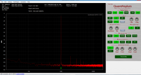
Connect 1000 pF to the output to simulate a long coaxial cable and it will likely oscillate again.
The simulation gives no indication of oscillations (even with 10000pF) when gate stoppers of 470ohm are applied (for the follower and the PSU cascode).
An offset large a this, some drift and strange noises are hints to parasitic oscillation in many cases.
Mosfet Vgs values will vary, matching may be needed. The offset (after matching) can be trimmed by adding a resistor(Rs) in series with the mosfet source. Resistors up to 100ohm (I did not check larger values) do not show in the FFT analysis.
Computer simulation has little to do with the real circuit.The simulation gives no indication of oscillations (even with 10000pF) when gate stoppers of 470ohm are applied (for the follower and the PSU cascode).
Computer simulation has little to do with the real circuit.
Ahhh... you are telling me.
But it has something to do with the real thing, else why is simulation used at all?
If not for simulation, this circuit may have never existed.
Maybe a more positive contribution will be more helpful
")
Last edited:
Maybe a more positive contribution will be more helpful
JG talked about oscillation. That is the real thing and does not show up in simulation.
Frans, what kind of contribution are you looking for?
OK, some contribution.
I have a look at your right hand circuit in post 9981.
Mosfets 7 and 9 have the same n-channel designation, but different polarity in the diagram.
But it is not the same on the negative side. Two ZVP3306 (8 and 10) are shown, p-channel from the datasheet.
I can not read the diagram in 9986, it is too small, but may be the same.
It is a small error anyway but it can be confusing.
OK, some contribution.
I have a look at your right hand circuit in post 9981.
Mosfets 7 and 9 have the same n-channel designation, but different polarity in the diagram.
But it is not the same on the negative side. Two ZVP3306 (8 and 10) are shown, p-channel from the datasheet.
I can not read the diagram in 9986, it is too small, but may be the same.
It is a small error anyway but it can be confusing.
The mosfet's are ZVN and ZVP 3306. As soon as Joachim is done testing (we are testing a new offset canceling solution) I will post a 'final' schema and .asc.
Last edited:
Frans, what kind of contribution are you looking for?
Any
maybe I barked a bit to loud, but most of the time I do not bite. The thing is I have a lot of time invested in this buffer and ... you know The offset trim works.
I have now put a 47 Ohm resistor in the source of the N-Channel output MosFet.
The rest i could trim with the negative CCS.
Offset is around 2mV, stable.
Then here the 'final' version
Attachments
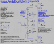
FdW asked for my contribution.
We see in post 10013 the edited and final version
of the right hand circuit in post 9981.
http://www.diyaudio.com/forums/analogue-source/154210-mpp-999.html#post4005947
This is a full feedback two stage amplifier.
For purpose of analysis the bootrapping mosfets M9 and M10 and
their associated components can be left away and replaced by a short.
Input transistors Q7 and Q8 work in common base mode.
They have high open loop gain because of
- current source load J5, J6 and
- high input impedance of the second stage M7, M8.
Output transistors M7, M8 are source followers.
Output is connected to the negative input (bases of 7,8)
as known from an opamp buffer, so the resulting voltage
gain is 1 and the input impedance goes up (it would be
as low as Ut/2Ic with a common base input without feed-
back). Q9 and Q10 are a short for ac, nicely coupling the
output to the negative input while preserving bias for the
input stage.
A desirable feature of this circuit (although not absolutely
mandatory with mosfet output) is the bias stabilization
performed by Q9 and Q10. Bias and residual (small) offset
may be adjusted by varying source resistors of J5 and J6.
The whole thing is bootstrapped by M9 and M10 and
associated circuitry. At this point two coupling caps C9,
C10 are required. If you want to avoid these, R32 and
R34 can be replaced by voltage sources and / or R31
and R33 by current sources, adding even more complexity.
With some resistors added, the gain can be increased,
giving a fine line stage. If preferably biased in A/B it may
also be a power amp output stage (leave away the boots-
trap transistors for this purpose).
It performed good in sim, no idea why it blew up ..
Last edited:
God is in the details and you can not sim god.
Call it a coincidence.
The day we can 100% sim we can direct play the music into the head.
We could do a macro analysis and a Monte Carlo but then variables get too much to solve that in time, even on a huge computer.
See the problem with weather.
Building is then the better option.
Anyway, sims got more powerfull and usefull but it also needs a master mind to use it on purpose.
So sim is not sim.
Whereas a rose is still a rose.
Last edited:
Thanks for explaining the circuit from your kind of view.
Is your view different?
Reminds me to a small boy in NYC, selling roses:A rose is still a rose.
"This is no flower - it's a rose!"