Parts list for beta board:
8 OP27
2 BD135 or equivalent
2 BD136 or equivalent
2 47R [carbon, provided in beta kit]
2 47R adjust to match cartridge impedance
4 220R
8 1k
2 ~1k adjust for desired gain
4 2k2
8 15k
6 33k
2 110k match
2 768k match (750k when using 2.9 nF rather than 3 nF for C2)
8 1 nF (match to 1x1 nF C1, 3x1 nF C2) [mica, provided in beta kit]
2 4.7 uF Black Gate N or substitute
20-24 100 uF/25V/2.5 mm lead spacing
4 1000 uF/25V/5mm lead spacing
8 8pin DIL sockets, optional
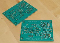
I spent a few hours today putting it together:
1. It works. No noise or hum. No obvious problems.
2. Yay!
3. Too early to do any evaluation, but definitely promising. It's different enough from the others than I'm going to have to careful...
An externally hosted image should be here but it was not working when we last tested it.
An externally hosted image should be here but it was not working when we last tested it.
An externally hosted image should be here but it was not working when we last tested it.
1. It works. No noise or hum. No obvious problems.
2. Yay!
3. Too early to do any evaluation, but definitely promising. It's different enough from the others than I'm going to have to careful...
The only thing that needs to be addressed immediately is the voltage output ended up half the value I expected. My phonoclone is now running at +/- 5V rather than +/- 10V intended.
That was because I was an idiot and ignored what Werner wrote earlier:
"The reference voltage (voltage between C4 and R4) is (approximately, ignoring R6) Vin * (R1||R2) / (R4+R5+R1||R2)
I dunno how I missed that. I'll update the schematic values to sort that out shortly.
That was because I was an idiot and ignored what Werner wrote earlier:
"The reference voltage (voltage between C4 and R4) is (approximately, ignoring R6) Vin * (R1||R2) / (R4+R5+R1||R2)
">Rather (R1//R3) / [(R1//R3)+R4+R5+R6]
I dunno how I missed that. I'll update the schematic values to sort that out shortly.
Thanks Richard,
I'm going to put together a mouser parts list for this - when I have it done I will send it on to you. I'll aim for 1% metal film and maybe tighter on the RIAA parts. I need to check out my stock and see if I have some blackgate non-polar... I've a bad feeling about that one. Have you any preferences yourself for this cap other than the blackgates? And what kinda of capacitance can we get away with?
I will probably order parts after Christmas and then have them in early January. I intend using my existing raw dual mono supply into these boards so will probably stick them into the box I have your BE boards in...
Thanks again,
Fran
I've recovered from the panic attack of yesterday. Well, for a start, I did listen to Werner; my calculations were right. The reason my output voltage was half what I expected was due to a number of small omissions and mistakes that unfortunately all summed in the same direction.
1. I underestimated and then neglected the voltage drop across R9 and R10. The actual voltage drop is ~1 V for every 100 ohms. I'd intended for a 1 V drop, but set 220 ohms in the circuit and, since I didn't have 220 ohms, used 300 ohms. So my V+ was 3 V less than I had anticipated.
2. I neglected the leakage through the filter capacitors C8-11. Of course the current is really small, by my estimate <1 uA, but it's enough to drop the reference voltage by 40 mV or so, which, in turn, means the output voltage was just over 1 V lower than I expected.
Knowing this, it's easy enough to change the values to get a higher output voltage. It's important though that output not get too close to V+. I'd feel comfortable leaving the positive output at least 4 V below the V+, though 3 V below is still probably OK.
So bearing that in mind, and trying to keep all the values as standard as possible, I suggest:
R9-10 = 100 ohms (for 1 V drop)
R11-14 = 22k (25k for 10 V output)
R15-18 = 2.2k (1/10th of R11-14)
R19-20 = 75k (30x R15-18)
An alternative configuration, giving almost the same result:
R9-10 = 100 ohms (for 1 V drop)
R11-14 = 10k (12k for 10 V output)
R15-18 = 1k (1/10th of R11-14)
R19-20 = 33k (30x R15-18)
For an input V++ of 17 V (about what can be expected from 12 VAC secondaries), the output is 12 V. Some people prefer to run the phonoclone at slightly lower voltage, and this can be most easily achieved by increasing R11-14 as noted above. (rule of thumb: a 10% increase reduces the output voltage by 10%)
An externally hosted image should be here but it was not working when we last tested it.
Attachments
Addenda for the above: R6 is 768k if you use C2=3 nF, 750k if you use C2=2.9 uF.
Here's the revised generic schematic for the Xreg, which looking at the way things are going, I will be using as a default circuit block element in the future.. headphone and preamp circuits being obvious targets. I don't think I could go back to LM7812's ever again...
Here's the revised generic schematic for the Xreg, which looking at the way things are going, I will be using as a default circuit block element in the future.. headphone and preamp circuits being obvious targets. I don't think I could go back to LM7812's ever again...
An externally hosted image should be here but it was not working when we last tested it.
Just for anyone else who is following this and thinking especially of the beta builders, I have a mouser BOM done for this, but have delayed posting it here until some final tweaks are done and RJM is happy with the circuit. Everything is in stock and available so there should be no hassle ordering it. Total from mouser excl shipping is about USD75, but that includes the mica caps that RJM is sending out to beta builders (cost is about USD20 from mouser) and also 2 wima MKP4 4.7uF caps for C3 at about USD11. So if you have your own source for these, that brings the cost down to the USD40-50 region.
Whats included is the stuff you need to fill the boards, transformers, cases and so on you need to add in to the mix.
Fran
Whats included is the stuff you need to fill the boards, transformers, cases and so on you need to add in to the mix.
Fran
The phonoclone boards have always had two sets of pads for the output coupling cap C3. The small set is 2.5 mm, and will fit the Black Gate N 4.7 uF / 50 V or the nonpolar Nichicon Muse equivalent. The larger set are spaced 22.5 mm apart, and were originally meant to fit the Wima MKP 4 2.2 uF part.
It is available in both 100 and 250 VDC varieties:
http://www.wima.de/EN/mkp4ue.htm
2.2 uF was always the target value for C3, not 4.7 uF. It only ended up being 4.7 uF because the Black Gate N came in that value.
Of course you can jury rig anything, but 22.5 mm lead spacing will look neat and tidy.
One more design note: the Eagle files show TIP40/41C transistors, which are Pin 1 : base, pin 2: collector, pin 3: emitter. The BD135,7 series are the reverse, Pin 1 : emitter, pin 2: collector, pin 3: base. When using BD transistors, rotate the transistor by 180 degrees so that pin 3 goes in the pin 1 position as denoted on the silk screen.
There is no current limit built into the xreg circuit. Shorting the outputs - or hooking it up to excessively massive capacitors - will almost certainly destroy the pass transistors.
Parts list, based on Fran's BOM:
R1 10R
R2 1K
R3 2K2
R4 2K2
R5 110K
R6 768K
R7 75K
R8 47R
R9 100R
R10 100R
R11 22K
R12 22K
R13 22K
R14 22K
R15 2K2
R16 2K2
R17 2K2
R18 2K2
R19 75K
R20 75K
C1 1nF
C2 1nF x 3 in parallel
C3 4.7uF blackgate N or 2.2uF film
C4 1000uF/25V
C5 1000uF/25V
C6 100uF/25V
C7 100uF/25V
C8 100uF/25V
C9 100uF/25V
C10 100uF/25V
C11 100uF/25V
C12 100uF/25V
C13 100uF/25V
C14 100uF/25V
C15 100uF/25V
C16 100uF/25V
C17 100uF/25V
IC1 Analog devices OP27 or TI OPA27
IC2 Analog devices OP27 or TI OPA27
IC3 Analog devices OP27 or TI OPA27
IC4 Analog devices OP27 or TI OPA27
Q1 npn BD135,137,139 or TIP41C
Q2 pnp BD136,138,141 or TIP42C
!BDxxx are ECB pinout, opposite to TIPxx BCE pinout!
- Status
- This old topic is closed. If you want to reopen this topic, contact a moderator using the "Report Post" button.
- Home
- Source & Line
- Analogue Source
- Phonoclone 3