"Isolate the op amp from the capacitance of the transitor base, right?"
More like ensuring that the transistor base never sees an inductive
drive impedance.
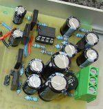
BTW, here's mine, including the rectifier and emitter-follower pre-regs. There are also SMD parts on the other side of the board.
I like the idea of crosscoupling the Vrefs, although it gets a bit costly once you employ really low noise (expensive!) references.
More like ensuring that the transistor base never sees an inductive
drive impedance.
BTW, here's mine, including the rectifier and emitter-follower pre-regs. There are also SMD parts on the other side of the board.
I like the idea of crosscoupling the Vrefs, although it gets a bit costly once you employ really low noise (expensive!) references.
Attachments
Time to put what I have so far up for public comment. You can click on the image to see a larger version.
I've shown the circuit in a slightly odd way: please note that the non-inverting terminals of both op amps are grounded. The numbers by the ground symbol indicate the order in which the grounds should be connected to each other. For non-Eagle users: the "X" symbol indicates a physical connection to the outside, an input or an output. The -> arrows are internal : "-> V-" connects to all the other sections of the schematic marked with the same label. The inverted "T" GND is an internal ground indicator in the same manner.
See if I'm on the ball with the maths:
The gain of the op amp stage is R2 / (R1+R3) = 68/2 = 34
The reference voltage (voltage between C4 and R4) is (approximately, ignoring R6) Vin * (R1||R2) / (R4+R5+R1||R2) = Vin * 500 / 20500 = Vin 1/41
The output voltage is Gain * Reference = Vin 34/41 or 83% of the input. e.g. input 18 V output 14.9 V.
* Re. your schematic, the odd feedback loop and the unsymmetrical circuit really threw me at first. I see it now: single, highly filtered reference, noninverting for the positive output, inverting for the negative output, both configured for a gain of 2. Earlier, I missed the fact that the second op amp was inverting... your "Looking more and more like mine now" comment makes more sense now...")
* Was there any particular reason to choose the BD137 series of transistors? I'm wide open to suggestions.
* Comments, suggestions, and error-reporting welcome.
An externally hosted image should be here but it was not working when we last tested it.
I've shown the circuit in a slightly odd way: please note that the non-inverting terminals of both op amps are grounded. The numbers by the ground symbol indicate the order in which the grounds should be connected to each other. For non-Eagle users: the "X" symbol indicates a physical connection to the outside, an input or an output. The -> arrows are internal : "-> V-" connects to all the other sections of the schematic marked with the same label. The inverted "T" GND is an internal ground indicator in the same manner.
See if I'm on the ball with the maths:
The gain of the op amp stage is R2 / (R1+R3) = 68/2 = 34
The reference voltage (voltage between C4 and R4) is (approximately, ignoring R6) Vin * (R1||R2) / (R4+R5+R1||R2) = Vin * 500 / 20500 = Vin 1/41
The output voltage is Gain * Reference = Vin 34/41 or 83% of the input. e.g. input 18 V output 14.9 V.
* Re. your schematic, the odd feedback loop and the unsymmetrical circuit really threw me at first. I see it now: single, highly filtered reference, noninverting for the positive output, inverting for the negative output, both configured for a gain of 2. Earlier, I missed the fact that the second op amp was inverting... your "Looking more and more like mine now" comment makes more sense now...
* Was there any particular reason to choose the BD137 series of transistors? I'm wide open to suggestions.
* Comments, suggestions, and error-reporting welcome.
> The gain of the op amp stage is R2 / (R1+R3) = 68/2 = 34
The gain is -R2/R1. The opamp is not aware of R3.
> The reference voltage (voltage between C4 and R4) is (approximately, ignoring R6) Vin * (R1||R2) / (R4+R5+R1||R2)
Rather (R1//R3) / [(R1//R3)+R4+R5+R6]
> * Was there any particular reason to choose the BD137 series of transistors? I'm wide open to suggestions.
Yes. It's the most widely-available medium power transistor over here.
You can buy them at the grocery store.
Werner said:> The gain of the op amp stage is R2 / (R1+R3) = 68/2 = 34
The gain is -R2/R1. The opamp is not aware of R3.
Surely the gain is -R2/ (R1+Z) where Z is the output impedance of the previous stage, which in this case is the voltage divider that has an output impedance at DC of approx. R3?
My mistake, I double dipped: Counting R1 as part of the voltage divider network, I should not have then counted the network impedance towards the op amp gain.
Fix: change R2 to 33k.
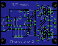
Most recent update of the Phonoclone 3 files attached. (capacitors C1 and C2 replaced with pads only as my CD silver mica caps have thick leads that don't fit in any of the standard Eagle caps in the build in libraries, and I'm too lazy to make a new part.)
Fix: change R2 to 33k.
Most recent update of the Phonoclone 3 files attached. (capacitors C1 and C2 replaced with pads only as my CD silver mica caps have thick leads that don't fit in any of the standard Eagle caps in the build in libraries, and I'm too lazy to make a new part.)
Attachments
Werner said:
@d to the g
You'll have to download and install Eagle www.cadsoftusa.com to view and manipulate the files. You may need the latest version, 5.3, I'm not sure.
When I say I'm trying it was more in reply to trying to follow, not trying to d/l the files. This circuit stuff doesn't come at all naturally to me.
I wondered at the time if I had miss-interpreted your post...
I don't think reading schematics comes naturally to anyone. Like reading sheet music, it takes practice. Plus there are some shorthand notation being used in the Eagle files here that are probably not intuitively obvious.
I'll take a stab at running though the Xreg circuit:
The raw voltage comes in at V-IN and V+IN. There is a filter capacitor C1/C1A that together with the total current draw of the load+regulator circuit elements, defines the initial ripple voltage.
The filtered voltage connects through the V++ and V-- "wormholes" to the collectors of the pass transistors Q1 and Q2.
The op amps are connected through the V+ and V- "wormholes" back to the main voltage filtered by the RC stage R6/6A and C2/2A. The op-amp power pins see about 10 times less ripple, and much less high freqency noise than the pass transistor.
The voltage powering the op amp is filtered and reduced by a two stage RCRC filter, R5/5A,R6/6A and C3/3A,C4/4A to generate the reference voltage. Its not an absolute reference, but the time constant is less than 1 Hz so it varies very slowly, essentially remaining "quiet" over the audio bandwidth and beyond.
The voltage amplifier is a textbook inverting configuration, but with the pass transistor inserted into the feedback loop. The output voltage is equal to the reference voltage multiplied by the gain, set as -R2/R1 and -R2A/R1A.
There are only a few oddities compared to your typical voltage regulator:
-The op amp is powered from split supply rails.
-The op amp is configured as an inverting amplifier, and takes the reference voltage generated from the opposite voltage rail as the one it regulates.
-The reference voltage is a fraction of the input voltage V+IN V-IN, not an absolute value because a filtered voltage divider provides a reference voltage, rather than a zener diode or precision reference.
The way the circuit "works" is as follows: the output is going to be equal to the reference voltage times the gain. For an 18 V input the op amp input sees about 450 mV at the input, 450 mV which is almost completely free of noise and ripple, and multiples that by -33 (R2/2A is 33k remember) to give -15 V, or 15 V from -450 mV for the positive rail.
The circuit is going to try to hold that 15 V constant no matter what the load does, over the bandwidth the circuit operates - in this case about 250 kHz - within the limit of the max current the transistor+raw voltage input can provide.
Thanks RJM!
Will you update the Phonoclone in your homepage?
I've just changed to "Benz Micro MC Gold" and start to build Phonoclone, since I'm not very familiar in electronics, can I ask a simple question?
What resistor control the gain, and what's the "safe" value should I use? Since VSPS, my M-Audio Firewire Audiophile got clipping all the time (with VSPS default) and I need to lower the input.
Thank you for sharing your work with us, arigatou.
johnsonlam said:What resistor control the gain, and what's the "safe" value should I use?
The basic phonoclone circuit is unchanged from before, so all the information regarding how to set the gain can be found on the existing Phonoclone page.
To reduce the gain change R2 from 1.5k to some lower value between 500 ohms and 1.5k.
/R
rjm said:To reduce the gain change R2 from 1.5k to some lower value between 500 ohms and 1.5k.
/R [/B]
Thanks rjm.
Sorry I'm totally nuts to mathematics and I don't know how to calculate (please forgive my stipidity).
I guess there're people like me, maybe you can change the phonoclone's R2 description to the quote above, to make it more clear.
Thanks again.
It's easy to order your own from Olimex though. Just complete the following form and mail it to fastpcb@olimex.com. You don't need to send any Eagle files, the "as Purchase Order RM271108" part below tells them to use the working files they made for my order instead. "1 pc" below gets you two boards, one for each channel. If you want extra sets, edit it to 2 pcs, 3 pcs etc...
*****
1. Name:
(your name)
2. Company:
none
3. Billing address:
(address)
4. Shipping address:
(address)
5. Shipping option:
airmail
6. Order:
1 pc "DSS (Phonoclone_30n_final.brd x2)" as per Purchase Order RM271108
*****
1. Name:
(your name)
2. Company:
none
3. Billing address:
(address)
4. Shipping address:
(address)
5. Shipping option:
airmail
6. Order:
1 pc "DSS (Phonoclone_30n_final.brd x2)" as per Purchase Order RM271108
- Status
- This old topic is closed. If you want to reopen this topic, contact a moderator using the "Report Post" button.
- Home
- Source & Line
- Analogue Source
- Phonoclone 3