Also, Salas, when I hooked up the raw supply to the reg, I connected the raw ground to Force negative. That is right isn't it?
Also, the ground is floating, i.e. not connected to earth, since it is on a breadboard.
Doug
Yes that is right.
Floating GND or not its no make or break condition for getting it running.
Hey Guys,
I am sure I switched the drain and source when I wired the MOSFETS.
Going to change them now.
Doug
Here is the part where B. Spears enters the scene and sings ooops!
")
Update:
After fixing the MOSFET pin wiring,
1. I have voltage in and out. Didn't have good solder joint at Vin turret. Doh!
2. It does't regulate. Vin = Vout (39.5 volts) regardless of pot setting from min to max R.
3. LEDs light up, although the third one is not as bright as the other two.
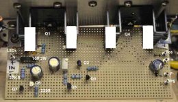
3. Read some voltages at MOSFET Pins:
For Q1, gate = 34.9 V source and drain = 39.4 V
For Q4 gate and source - 39.4 V, Drain = 0 volts.
My probe slipped, briefly shorting S and D on Q4.
Any suggestions.
After fixing the MOSFET pin wiring,
1. I have voltage in and out. Didn't have good solder joint at Vin turret. Doh!
2. It does't regulate. Vin = Vout (39.5 volts) regardless of pot setting from min to max R.
3. LEDs light up, although the third one is not as bright as the other two.
3. Read some voltages at MOSFET Pins:
For Q1, gate = 34.9 V source and drain = 39.4 V
For Q4 gate and source - 39.4 V, Drain = 0 volts.
My probe slipped, briefly shorting S and D on Q4.
Any suggestions.
Salas: do you actually listen to Brittany Spears?
I was watching rather than listening when the odd clip was on TV. She had kinda "rounded" musical culture that I tend to appreciate in female artists.
FdW: I don't understand.
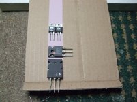
If you remove the white areas of the PCB then air can move freely along the fins of the heat sink and then it will be able cool better.
Attachments
Sorry off topic cant post picture on PM
Sandro, cheers mate! That hard to find strip will come handy for my TSSA I gather stuff for.
I'm back.
I misspoke earlier; It is actually the first LED that looks dimmer. Each drops 1.8-1.9 volts. 5.65 V all together.
R4 shows 20.5 V drop.
R5 shows 0.6 V drop.
Yes I have a spare Q2.
FdW: got it now thanks. that makes sense.
Doug
Q3 change fixed a number of voltages. Before changing Q2 which is inline loading it and if there is a hit in the error amp they form they usually die together, please look is there completed resistive path from Q5's drain through R7 and trimmer to V+ force AND sense when not tied together at a dummy load? What value is the dummy load again?
AAARRRGGGHHHH
OK. Replaced Q2 before I got your last message Salas.
Vin now reads 21 V instead of 40. (Voltage sag??) Diodes read OK in raw supply.
Anyway, Q1 now gets warm. Q4 still cold.
Pot resistance measures 0 to 4.7 kohm.
Q5/R7 node to Force (+) is big, about 8 megohm or OL.
Q5/R7 node to Sense (+) goes from 3.3 kohm to 8 lohm depending on pot setting.
V drop across R4 is 20.4 V
V drop across R5 is 0.55 V
Vdrop across R7 is 2.7 V
V drop across R1 is 2.2 V
Vin about 21 V
Vout with load (500 ohm) is 3.5 V
Vout with no load is 10.8 V
Q1 G to S = 3.3 V
Q4 G to S = 3.4 V
Q2 G to D = 3.4 V
Q3 B to E = 0.7 V
Q5 G to D = 0.7 V
Q6 B to E = 0.6 V
Q7 B to E = 0.54 V
What next boss?
- Home
- Source & Line
- Analogue Source
- Simplistic NJFET RIAA