What about this:
P.S. Sorry for off topic.
Too much gain for a wise system gain structure I would suppose. But if you have a SSHV reg which is adjustable, a few favorite valves, and some leftover passive components you can experiment with potential circuits till the cows come home. A line valve stage is simple, low components count usually, and fun to play. Big glowing, all parts hefty to hold and put together.
P.S. 165V 40mA setting on the reg should suffice for that cct you posted.
I have on hand:
50K Noble can I use after circuit for volume pot, or need 100K or more?
1 Tx 240V & 8.5V from old Audionte DAC 2 can I use it?
As tubes I have on hand 2 tubes matched pairs of:
E88CC Siemens OB NOS gold pin (the best for everybody)
6922 Sovtek matched for Rod Elliot (Altavista Audio) are the best current manufacturer ultra low noise
E88CC / 6922 NOS Russian ultra low noise (mine favorites)
Sorry for off topic.
Last edited:
Power comes from outboard psu into a 5 pin XLR.
Inside riaa case, power goes from XLR to the shunt using 2 core shielded cable. Shield is used to connect shunt to star gnd at XLR. Two inner wires carry (+) and (-).
From shunt to riaa board I use two cables:
Sense (+) and (-) are connected using single thin coax.
Force (+) and (-) connected using the same mic cable as before.
Remenber that I had no problem with my previous v1 shunt.
Beautiful I must say. There are wide distances from + to 0 due to big parts, there can also be a gremlin in the CCS cascode or CFP arrangement, but those things can't be reliably guessed at. The best method is we standardize a layout for the regs on dummy load with the help of an oscope, then we put them in, check again with real load, we know power is clean, then we change things about helping loop area to be tighter if the whole build presents hum sensitivities. This is 56dB gain, it will not give us slack. But you wrote its very nice for hum now with the Klotz shielded power runs. That hints towards loop area pick up. It would not change oscillation. V1 had 5mm pin distance electrolytics was much more together for +/0 in its output and bypass too.
Volume pot value? 50K or 100K after circuit or before circuit? current for heater 6.3V?
Isn't there any comment or psu arrangement where you found that CCT? Anyway, I would use a 50K log on input. Those novals need 365mA @ 6.3V each. The top one's heater must float on some B+ potential divider since there is 50V max cathode to heater spec in those.
Isn't there any comment or psu arrangement where you found that CCT? Anyway, I would use a 50K log on input. Those novals need 365mA @ 6.3V each. The top one's heater must float on some B+ potential divider since there is 50V max cathode to heater spec in those.
I din't see nothing, link:
6DJ8 / ECC88 / Symmetrical SRPP Tube Preamplifier Schematic
If you will prefer can continue by pm?
Well, I already built six v12 with EL output cap with exactly the same layout and those work perfectly without any hum. But the fullfim is much better in terms of dynamics, detail and speed.
With the klotz cable, hum is only aparent when at full power without signal but I need to get rid of it (or at least determine it´s precise origin) Maybe the big output cap is acting like an antena.
What is CFP arrangement ?
I decided to invest in an oscope.... Is this suitable ? VELLEMAN SA - HPS10 - OSCILLOSCOPE, HANDHELD, 10MHZ VELLEMAN SA|HPS10|OSCILLOSCOPE, HANDHELD, 10MHZ | Farnell Portugal
I chose it for the lowest cost because I am now quite short in tim€
Last edited:
In the riaa board, blue is GND and brown (red in real life.. camera to blame) is (+).
Maybe I should try to interlace those lines to minimize the loop area....
The top terminal block is (-) and the lower one is (+)
What you see is a solder point needed to connect sense wire to the upper terminal block (-).
Maybe I should try to interlace those lines to minimize the loop area....
The top terminal block is (-) and the lower one is (+)
What you see is a solder point needed to connect sense wire to the upper terminal block (-).
What is CFP arrangement ?
I decided to invest in an oscope.... Is this suitable ? VELLEMAN SA - HPS10 - OSCILLOSCOPE, HANDHELD, 10MHZ VELLEMAN SA|HPS10|OSCILLOSCOPE, HANDHELD, 10MHZ | Farnell Portugal
I chose it for the lowest cost because I am now quite short in tim€
Its the compound pair of BJT buffer transistor and output Mosfet. Those are good to be very intimate in layout.
A very practical handheld instrument with many calculating and holding functions, yet only 2MHz and 100VDC in. If you evolve your troubleshooting skills and want to play with tubes maybe you will outgrow it. Of course it will show a gross disturbance on DC but you could browse European Ebay sites for 230VAC import hassle free used desktop CRT full scopes for under EUR100 too before you buy.
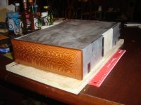
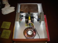
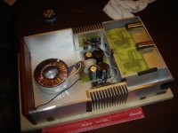
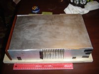
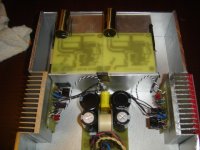
While waiting for parts for the RIAA section, I thought it would be a good time to build the chassis. Attached are photos of chassis taped together for review. Still some fitment to complete, but the layout can be seen. The chassis is made of aluminum with a wooden faceplate for cosmetics. The RIAA stage will be installed in a secondary aluminum box seen within the main chasis. Power will be fed from the shunt regs through a couple of small holes. The Force and sense wire will be Belden Blue Hose (shielded two conductor) 22awg cunductors. It is good wire with low capacitance 17pF/ft.
Inside the RIAA shield, the output caps will solder direct to the RCA connectors. The input wire will be cardas two conductor shielded from the RCA post to the board. All runs will be less than 100mm. I put the caps and board on top of the inner box for reference.
Since the main chasis is completely metal enclosed, I did not include the shunt reg in the inner box. My only concern now is the magnetic fields from the PT and some EMI (AC mains) from the input side of the PS board seen in the center of the chasis. I have tested, using the oscilloscope, this arrangment and I still cannot detect any ripple/noise from the shunt regulator. With the RIAA further shielded I feel that 60 Hz pick-up from the AC mains would be minimal if at all.
Any thoughts or improvements or a critical flaw which I can correct before I start final assembly? I would prefer not to go bigger on the case, and for right now I want to keep the unit as a single chassis.
Thanks for your opinions, all are welcome.
Attachments
The RIAA stage will be installed in a secondary aluminum box seen within the main chasis.
Nice idea, but aluminum as shield has a very limited effect (unless 1/2" thick).
It's most probably better to use just a thin sheet of mild steel vertically, between the two heatsinks.
My 2c
the wide loop formed by the power lines will act as a receiving aerial for electromagnetic radiation.In the riaa board, blue is GND and brown (red in real life.. camera to blame) is (+).
Maybe I should try to interlace those lines to minimize the loop area....
The wires show the problem. The spacing of the tapping points show the problem.
The circuit formed by the supply lines, flow and return, must be small loop area. This philosophy must also exist in the traces on the PCB.
How about if I make the box from steel? The AC mains will come from the back corner next to the RIAA boards. The idea of a piece of steel between the heat sinks is appealing as it is very simple but I am afraid it may not shield it from the power line noise.
Steel is quite effective even in small squares that must be connected to GND.
The tranny is a 2x18V 4amp connected in series from an old recycled project. It feeds a RCLC network. R=.75R (mostly for voltage control) C1=13,400uF L1 = 0.25mH C2= 24,000 uF. Caps are long life low ESR. Ripple per PSUDII is approx 100uV. It is undectable using my scope at 2mV/div. The rectifiers are MUR 100V 3A schotky's. I don't have a schematic on hand to post but it should be easy enough to draw one from the above info.
- Home
- Source & Line
- Analogue Source
- Simplistic NJFET RIAA