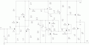
I'm starting this thread to describe some of the work I've done with simple single ended open loop JFET and MOSFET circuits with an RIAA preamp in mind for MM cartridges. The original work was inspired by the simple "Pacific" RIAA preamp. Quite a few bows and ribbons have been added to that basic design over the past couple of years, resulting in the circuit shown below. Bits and pieces of the rationale (and some of the intervening work) are covered in the threads "Open Loop Follies, Pt. 1" and "JFET SRPP RIAA Preamp".
The scope of this investigation was deliberately limited to simple single ended circuits using a single positive supply and N-Channel devices. The test bed for all iterations used an external +40V unregulated supply, feeding a +30V regulator located on the preamp circuit board. About halfway through my investigatiions, I decided to narrow the scope of the investigation still further to a preamp using domestically made (US) JFETs and MOSFETs, out of a mixture of curiousity and sheer cussedness.
No doubt there are other topologies that may work better than the one presented here. However, the thrust of this thread is to see how much can be wrung from a single-ended design using N-Channel devices. If you want to sing the praises of another topology, please start another thread and do your singing there. Also, this preamp was made specifically for MM cartridges or high output MC cartridges, and may not be the best approach for low output MC cartridges.
The final circuit is shown in the attachment below. What I'll do in the next few days is to describe the circuit rationale, starting with a very simple circuit, and adding pieces on gradually. Simulation results will be shown for each step.
Attachments
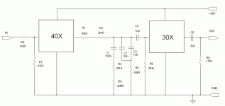
To start off with, the circuit is stripped down to a basic block diagram, reducing it to two gain blocks with a passive RIAA network in between. The first gain block is set at 40, the second at 30. This results in a gain of 40 dB at 1kHz, which suits the rest of my system pretty well. The next posts will talk about the approaches chosen for the first gain block, starting real simple and working up.
Attachments
The obvious gain block to start with for the first section of the preamp would be a simple common source amplifier. Since it's the first stage with a small input signal, it should use a low noise device.
A couple of other constraints apply as well. The quiescent drain voltage of the amplifier should be place somewhere near 1/2 the supply voltage, in order to ge the maximum symmetrical output voltage swing. This will help the amplifier to handle input overloads gracefully. Since this is the input section and the output voltage swing is still relatively small, you don't have to be a real fanatic about it. For example, 2V on the drain would be too low. Somewhere around 10-20V would be acceptable (15V or 1/2 the supply voltage would be perfect).
Next, you want to have a reasonable amount of bias current flowing in the JFET. This reduces noise somewhat, and also reduces distortion, as the signal current will be a small percentage of the bias current. In other words, the device characteristic won't vary too much as you're driving it. Again, this requirement is somewhat flexible - 50uA would be to low, while a few milliamps would be ok.
The device I'm using for starters is the Toshiba 2SK170, a low noise, high (relatively) transconductance N-Channel JFET. This is actually the device I started with when I first began this investigation. We'll keep with this device for the first three evolutionary steps, then look for ways to replace it.
The circuits shown in these steps will all be taken from Orcad simulations, and use the default device models availalable there. Actual devices generally be different from the simulator values in terms of Vgs, IDSS, and other parameters. The simulator allows one to quickly grasp the general features of a design. For those who follow such things, reltol was set to 0.0001, and step size was set to 20ns.
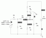
A simulation of a simple common source amplifier using the 2SK170 is shown below. A 1k resistor is placed in series with the input voltage source to approximate the resistance of a typical MM cartridge, and the 24k load resistor approximates the loading from a passive RIAA filter as used in my preamp at high frequency. With the component values shown, the gain is 38, pretty close to the target value of 40. Bias current in the JFET can be calculated from the voltage across the source resistor, and is 3.18 mA - not too bad. Calculated p-p current swing at 1mV drive is 0.076V/6k, or 12.6 uA p-p. The 24k load adds another 3 uA to this current, so the total current swing is about 15.6 uA, The signal current is about 0.5% of the bias current so one might reasonably expect the distortion to be pretty low. Quiescent drain voltage is 10.9V, which should allow enough voltage swing for anything short of a gross overload condition.
A couple of other constraints apply as well. The quiescent drain voltage of the amplifier should be place somewhere near 1/2 the supply voltage, in order to ge the maximum symmetrical output voltage swing. This will help the amplifier to handle input overloads gracefully. Since this is the input section and the output voltage swing is still relatively small, you don't have to be a real fanatic about it. For example, 2V on the drain would be too low. Somewhere around 10-20V would be acceptable (15V or 1/2 the supply voltage would be perfect).
Next, you want to have a reasonable amount of bias current flowing in the JFET. This reduces noise somewhat, and also reduces distortion, as the signal current will be a small percentage of the bias current. In other words, the device characteristic won't vary too much as you're driving it. Again, this requirement is somewhat flexible - 50uA would be to low, while a few milliamps would be ok.
The device I'm using for starters is the Toshiba 2SK170, a low noise, high (relatively) transconductance N-Channel JFET. This is actually the device I started with when I first began this investigation. We'll keep with this device for the first three evolutionary steps, then look for ways to replace it.
The circuits shown in these steps will all be taken from Orcad simulations, and use the default device models availalable there. Actual devices generally be different from the simulator values in terms of Vgs, IDSS, and other parameters. The simulator allows one to quickly grasp the general features of a design. For those who follow such things, reltol was set to 0.0001, and step size was set to 20ns.
A simulation of a simple common source amplifier using the 2SK170 is shown below. A 1k resistor is placed in series with the input voltage source to approximate the resistance of a typical MM cartridge, and the 24k load resistor approximates the loading from a passive RIAA filter as used in my preamp at high frequency. With the component values shown, the gain is 38, pretty close to the target value of 40. Bias current in the JFET can be calculated from the voltage across the source resistor, and is 3.18 mA - not too bad. Calculated p-p current swing at 1mV drive is 0.076V/6k, or 12.6 uA p-p. The 24k load adds another 3 uA to this current, so the total current swing is about 15.6 uA, The signal current is about 0.5% of the bias current so one might reasonably expect the distortion to be pretty low. Quiescent drain voltage is 10.9V, which should allow enough voltage swing for anything short of a gross overload condition.
Attachments
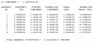
The attachment below shows the simulated distortion characteristics for the simple comon source amplifier just described. The results below shouldn't be taken as complete gospel, but can be used to look at the relative merit of a design. The THD shown is less than 0.01%, and consists almost entirely of second harmonic. This is typical of a single ended JFET amplifier at low drive levels. An actual device might exhibit somewhat higher THD, but the distribution of harmonics should be similar.
So far, so good. There are actual preamps out in the world that consist of two cascaded common source stages with a passive filter in between. The Pacific preamp is one example (a schematic is shown in the thread "Discrete Phono Preamp Designs?") . However there are other factors that must be considered in the gain block design for an RIAA preamp. I'll talk about those later....
So far, so good. There are actual preamps out in the world that consist of two cascaded common source stages with a passive filter in between. The Pacific preamp is one example (a schematic is shown in the thread "Discrete Phono Preamp Designs?") . However there are other factors that must be considered in the gain block design for an RIAA preamp. I'll talk about those later....
Attachments
Next thing to consider is the interaction of the input satge with the cartridge. Most MM cartridges have a high inductance (0.5 - 1H!), and are thus sensitive to the value of loading capacitance. This includes the connecting leads from the turntalble to the preamp, and also the effective input capacitance of the preamp itself. The 2SK170 has a Cgs of 30pF, and a Crss (reverse transfer capacitance of 6 pF. The Crss is multiplied by the stage gain of `40, so the input stage can pesent a capacitance of `270 pF to the cartridge, not even including the effect of the input cables. Thios means that one will be starting out with a loading capacitance that is probably greater than optimum, with no convenient way of trimming it down.
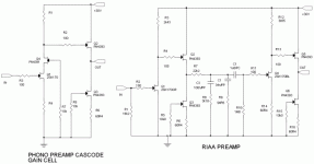
Adding a cascode stage to the input JFET reduces the multiplying effect of the input stage gain on the Crss by pinning the drain of the input (bottom) JFET at a constant voltage. The input device sets the drain current of the cascode stage. Cascoding can be accomplished by using a bipolar transistor, and there are some variations on the Pacifiic preamp that use this scheme. I prefer to use a simple sellf-biasing JFET cascode stage as shown in the attached schematic. The JFET placed on top of the bottom gain JFET sets the drain-to-source voltage of the bottom JFET. This voltage is set by the gate-to-source voltage (Vgs) of the top JFET at the bias current of the bottom FET. With this in mind , one chooses a cascode FET with an IDSS greater than that of the bottom FET, so it will running in the pinch-off region with a relatively high Vgs. I like to run the bottom FET of the cascode at a few volts to reduce the parasitic capacitances, yet not so high that the FET is operating in the region of exponential gate leakage current. This is important with the 2SK170, as the transition to exponential gate leakage current occurs at a relatively low voltage.
One good choice for a cascode FET is the PN4391. It has a relatively high breakdown voltage (40V), and a high value of IDSS. Used with a bottom FET drawing a few milliamps, it will bias that FET at 4-6V. The PN4391 is generally used as a switch or a chopper, but is also useful as a cascode. Its lower IDSS brother, the PN4393, has many uses as a linear amplifier. Both devices are readily available (fingers crossed).
The attached schematic shows a simulation of the cascode circuit described above. Operating voltages shown are very similar to real-life operation. A gate stopper resistor is included on the cascode FET to squelch any tendancy for spurious oscillation.
Attachments
The gain of the circuit is not materially changed by addition of the cascode, and is ~38.5 (31.7 dB). Distortion is not radically changed, either, though the even order components are slighly increased in magnitude. Simulated distortion profile is shown below, and should be used for indication purposes only, though the trend shown is encouraging.
Attachments
Next to consider is the loading effect of the passive RIAA. this load is variable, will the impedance falling as a function of frequency. The RIAA filter values are calculated assuming a stiff voltage source to drive the equalizatin netwoer. Driving the equalization network with a high impedance source will introduce error into the response curve. The output impedance of a common source amplifier is the parallel combination of the drain load resistor and the output impedance of the JFET at its given operating point.
One way to get around this problem is to use a buffer between the input stage and the RIAA network. This can be accomplihed in many ways - I chose to use an all-JFET source follower with current source loading. Utilizng the inexpensive and readily available PN4393. The imulation schematic and DC operating points are shown below. The buffer increases the overall gain of the circuit from 38.5 to 49, due to the elimination of the loading effect. If desire, one could compensate for this by lowering the value of the drain resistor on the input stage. This would also raise the drain voltage of this stage a bit, increasing the available output voltage swing.
One way to get around this problem is to use a buffer between the input stage and the RIAA network. This can be accomplihed in many ways - I chose to use an all-JFET source follower with current source loading. Utilizng the inexpensive and readily available PN4393. The imulation schematic and DC operating points are shown below. The buffer increases the overall gain of the circuit from 38.5 to 49, due to the elimination of the loading effect. If desire, one could compensate for this by lowering the value of the drain resistor on the input stage. This would also raise the drain voltage of this stage a bit, increasing the available output voltage swing.
Attachments
The attached picture shows basic schematic of the preamp I built using the principles outlined above. I liked it well enough to permanently ditch my Nikko Beta peamp. I lived with this circuit for a few months, and added a cascode JFET later to the input stage as outlined above. There's a lot of detail on this and a few other circuits in the old thread "Open Loop Follies Part 1". Two concerns remained, though. I wanted to try and build an good MM preamp using nothing but JFETs that I could easily order in the US. Also, I was concerned about distortion in the second stage, which operates at a much higher voltage swing than the first. More on this later.
Attachments
Those who are satisfied with things so far could build a modified Pacific preamp as shown here and a couple of other threads, with either JFET or bipolar cascode and buffering, and not do too badly. One remaining concern I had was with distortion in the second stage, which sees higher signal levels. Attached is a simulation of a second stage circuit trimmed for a gain of ~30 and driven to one volt output.
Attachments
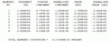
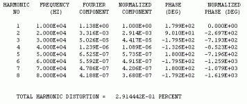
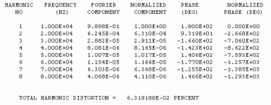
Attached here is the simulated harmonic profile of the second stage gain cell as described above. As one can see, the distortion is much higher than the input stage, though it is overwhelmingly second harmonic. The next couple of posts will show measures to recuce the second stage distortion and to replace the 2SK170 with more readily available devices. It turns out that both goals are attainable using similar measures.
Attachments
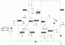
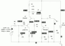
Next we look at the output stage to figure out how to get lower distortion and at the same time, ditch the 2SK170 for something available in the US without a lot of roaring and screaming. Hacking around with simulations in PSpice, I found that the best solution was to use a small signal MOSFET for the X30 gain output stage, and to bias it fairly hard. There are two requirements for the output stage that are not necessarily mutually inclusive. 1) x30 Gain 2) the drain voltage should be near 1/2 the supply voltage for maximum symmetric output swing. I found that if a separate current source was added to bias the gain FET indepent of the current going through the load resistor, one had a fair amount of impunity to juggle values to get the desired gain and drain voltge. In addition, the extra current pushes down the THD of the output MOSFET.
The circuit shown below used a ZVN3306A small-signal MOSFET. Two current sources (J2 ans Q2) were used. J2 passes current through M2 and R5, which are used to bias M1, as it is an enhancement mode device and needs some positive bias to run.Q2 provides extra bias to M1 that does not pass through load resistor R2, allowing one to set bioth gain and quiescent drain voltage of M1 to the desired values. The extra current is injected into the junction of J1 and the M1 drain, which is pinned to a relatively constant low voltage. Since M1 is pinned to a low VDS by J1, the power dissipation is well within the limits of the ZVN3306A. Quiescent current is 17m/A and VDS is 3.88 V, yielding a power dissipation of 66 mW.
J4 and J3 form a buffer to the cruel outside world. In the case of this RIAA preamp, the load is a law-faked volume control with a minimum imprdance of about 15k.
Attachments
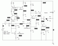
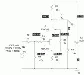
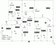
Last step - let's use the principles shown so far and ditch the 2SK170 in the input stage. The schematic shown below shows a possible circuit implmented in PSpice, using the J110. Other JFETs could be used as well. This exercise was not meant as a "buy American" bit of jingoism, but as an exploration in what could be done with parts readily available on the home front. No doubt a similar exercise could be conducted with European JFETs by some enterprising individual.
One more try to upload here, before I yell to admin. Attached is a simulation for an input gain cell using all the bows and ribbons/bells and whistles discussed so far. The FET of the day is the J110, normally a switch/chopper FET, but one that works quite nicely in the linear region, too. I also did a simulation using the J310 RF FET (not shown here). Results were similar, though the bias point was different. Bias current for the J110 in this simulaton was 8.6 mA. The J110 model available in PSpice has a transconduction about 2X that of the devices I've used so far. I've been using a bag of Vishay FETs purchased from Mouser. I may try using some Fairchild J110s I also have on hand, or try selecting devices with higher IDSS to work with, as I am getting about 10 mS transconductance with the FETs currently in my preamp. If I can get the 22 mS shown in the simulation model, that would be a pretty good match for the 2SK170 I'm trying to replace.
Attachments
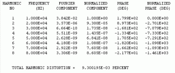
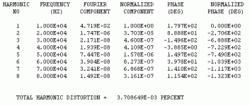
Here's the simulated distortion profile for the circuit just posted. THD is less than half that of the 2SK170 circuit with cascode and buffer at identical excitation levels. Harmonic distribution looks nice, too.
That pretty much covers the rationale behind the circuit I initially posted, which is on duty in my living room as I write this . Any questions or comments at this stage? The thread has been pretty quiet....
That pretty much covers the rationale behind the circuit I initially posted, which is on duty in my living room as I write this . Any questions or comments at this stage? The thread has been pretty quiet....
Attachments
The only thing left is to describe a rationale for selecting FETs to build the RIAA preamp I've described so far. This will take a bit, as this project started over a year ago, and was bootstrapped to completion by the impending Burning Amp fest of October 2007. This will probably mean building another board to recapture my thought train. Not a real hardship, as I wanted to select for a higher transconductance J110 anyway, and I have some new ideas regarding a cleaner on-board regulator inspired by the long-running "Blowtorch" thread.
The old chopper FETs I've been referencing (PN/2N 4391-4393 and others) are an interesting set of devices. They have medium transconductance and low gate-source and reverse transfoer capacitance, since they were o\riginally slated for high -speed switching applications.. Some fortuitous quirk of history also makes them relatively easy to find, though that could change at short notice. John Curl and others have been using similar devices since the '70s..
At any rate, I'm going dormant for a while as I repackage what I have and forge on. I'm surprised the usual pundits haven't been all over me...
- Status
- This old topic is closed. If you want to reopen this topic, contact a moderator using the "Report Post" button.
- Home
- Source & Line
- Analogue Source
- "All American" RIAA Preamp