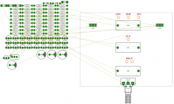
I have draw in Eagle Schematic APEX P30ZF preamplifier and have a few questions about using PCB connectors for power supply, input audio connector and out connection. And question about placement large components so that i can define other PCB components placements and later routing.And not to have hum or noise...so placement large main components it very important...
Questions:
1. For Power Supply (+24V GND -24V) it is ok to place OUT there or is better to leave it as is in PCB Layout posted above? Or what is recommended to place OUT connector? (+24V GND OUT -24V) or (+24V GND -24V)? Or OUT to put far away from power connectors (+24V GND - 24V)?
2. What type for Power Supply connectors is recommended? (Direct wire to PCB or using 3 pin connector with 5.08mm spacing between pins? Like Screw Terminal:
http://s3.amazonaws.com/emimg/Products/NN-149/1B.JPG
Or using 3 pin with header?
https://www.allelectronics.com/mas_assets/cache/image/4/4/4/1092.Jpg
3. Some idea where to place and route ground to minimize noise and hum (star ground or ground plane?)
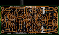
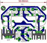
Here is alex_mm P30ZF layout that i need that these components needs to be placed in other direction...suggestions? How to imporeve placement?
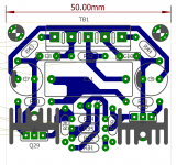
Here is picturs...first picture is my opinion how it needs to be positioned 10uF/100V MKT capacitors (C1,C3 and C11) and in front is 100k LOG potentiometer that will be later in case so connecting two potentiometers using wood will make volume on both modules (stereo) to increase or decrease....tranzistors in TO126 on left and right will have large heatsink like on alex mm layout (i im doing drawing of heatsink component in eagle footprint so that's why is not show in above PCB components placement)
So anyway please make your guide of what will be perfect components placement and routing to minimize noise and most important to make audio preamplifier functional.
Questions:
1. For Power Supply (+24V GND -24V) it is ok to place OUT there or is better to leave it as is in PCB Layout posted above? Or what is recommended to place OUT connector? (+24V GND OUT -24V) or (+24V GND -24V)? Or OUT to put far away from power connectors (+24V GND - 24V)?
2. What type for Power Supply connectors is recommended? (Direct wire to PCB or using 3 pin connector with 5.08mm spacing between pins? Like Screw Terminal:
http://s3.amazonaws.com/emimg/Products/NN-149/1B.JPG
Or using 3 pin with header?
https://www.allelectronics.com/mas_assets/cache/image/4/4/4/1092.Jpg
3. Some idea where to place and route ground to minimize noise and hum (star ground or ground plane?)
Here is alex_mm P30ZF layout that i need that these components needs to be placed in other direction...suggestions? How to imporeve placement?
Here is picturs...first picture is my opinion how it needs to be positioned 10uF/100V MKT capacitors (C1,C3 and C11) and in front is 100k LOG potentiometer that will be later in case so connecting two potentiometers using wood will make volume on both modules (stereo) to increase or decrease....tranzistors in TO126 on left and right will have large heatsink like on alex mm layout (i im doing drawing of heatsink component in eagle footprint so that's why is not show in above PCB components placement)
So anyway please make your guide of what will be perfect components placement and routing to minimize noise and most important to make audio preamplifier functional.
Attachments
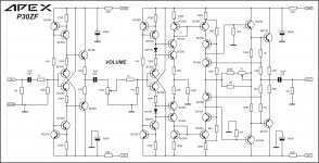
APEX make public schematic in this thread:
100W Ultimate Fidelity Amplifier
And alex_mm have designed nice pcb board posted above (middle attached picture)...i just want to design PCB in Eagle in my own way..but need some directions what needs to be done ok so that final product will be without noise and hum (gnd star)
I make this only for hobby (learning PCB Layout) and later building P30ZF Amplifier...so after i design pcb it will be made two copy of board (stereo) and published PCB layout...
As a first glance, I'd copy the layout as is, looks okay to me.
I think that you should ask these questions to AlexMM and Mile yourself in Mile's thread?
I would think that they would be the first people to ask then if you do not get your answers, then try another method.
I do question if this is intended for a stereo application, how do you plan to get both channels to track each other?
It is up to you to use the connector footprints or hard wire, it is application dependent. Sometimes you only use the connector on one end and hardwire the other end, to make dis-assembly/service easier.
- Status
- This old topic is closed. If you want to reopen this topic, contact a moderator using the "Report Post" button.
- Home
- Source & Line
- Analog Line Level
- PCB Placement Position Preamplifier