Does anyone know what topology was used in the George Wright WLA12/A line preamplifier? It uses a 6X5 rectifier, 6EM7 as a series high voltage regulator, and two 6SN7s for what his old website describes as the "voltage and driver stages."
Does "voltage and driver" stage have a particular meaning?
I'm trying to understand the differences between common preamp topologies (SRPP, mu follower, cathode follower, grounded grid, etc.), and the WLA12 is the only one I've ever heard. Trying to match experience with book learning here.
Thanks!
Jeff
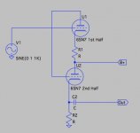
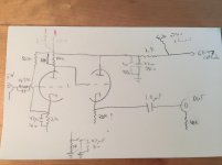
I started reverse engineering the WLA12 using photographs from the web and a resistor color code chart. As far as I can tell, the WLA12 does not conform to the usual VA/CF topology, but is more like an SRPP or mu follower.
That's because pin 6 (cathode of section 1) is connected to pin 2 (plate of section 2) by a resistor. Also pin 5 (plate of section 1) is directly connected to pin 1 (grid of section 2). Pin 5 has no other connections: the only connection to the B+ rail is at pin 2 (plate of section 2).
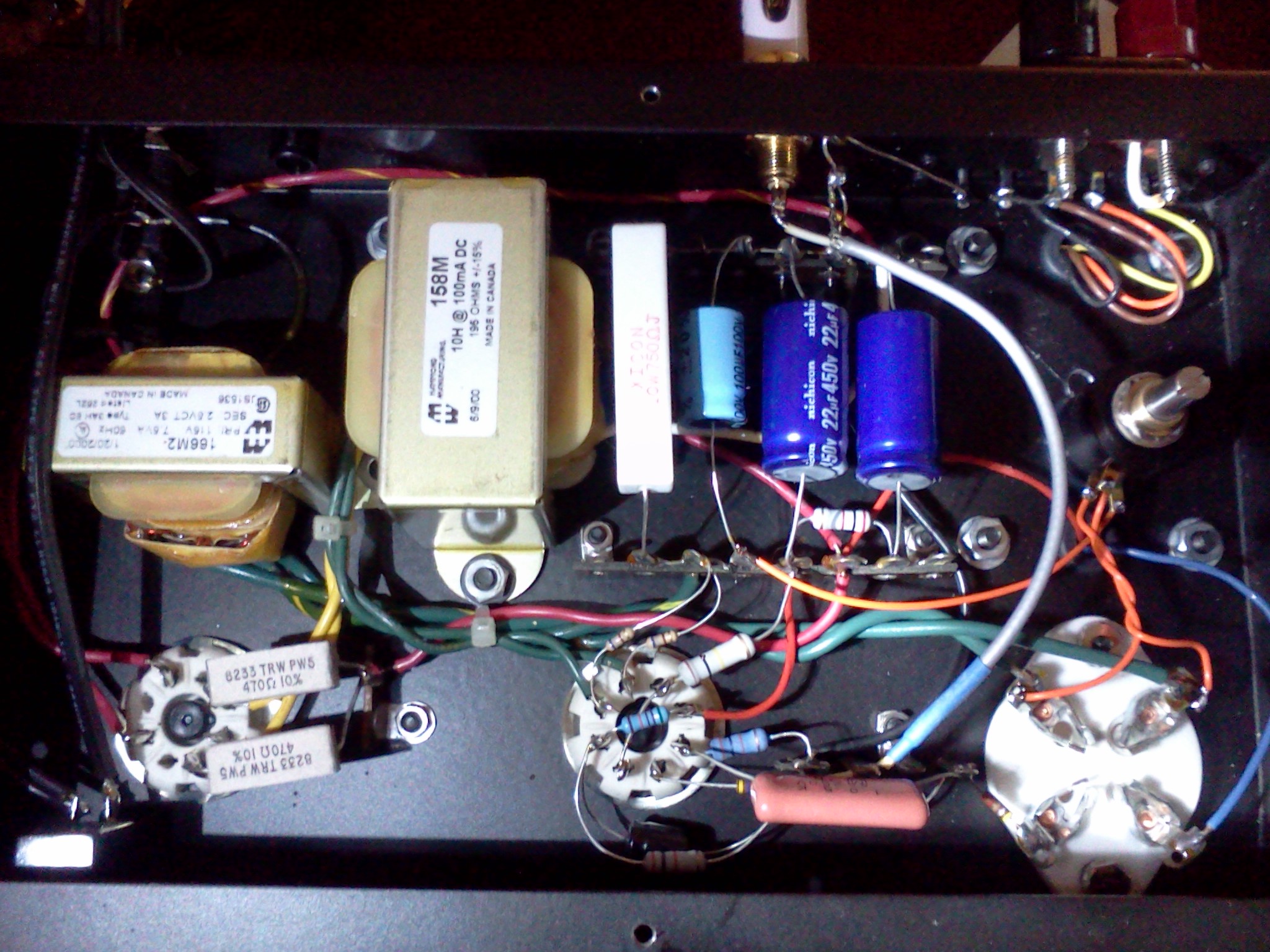
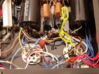
By my best reckoning, the basic schema (without component values yet) for the 6SN7 looks like the attached screenshot. I've included the 6SN7 pinout diagram and two of the pics I'm working from.
In the first pic, the 6EM7 regulator is on the left and one 6SN7 on the right. The second pic shows the two 6SN7s and the ALPS Blue Velvet volume pot, which connects to pin 4 (grid of section 1) with a paralleled resistor and capacitor.
Does this seem feasible?
That's because pin 6 (cathode of section 1) is connected to pin 2 (plate of section 2) by a resistor. Also pin 5 (plate of section 1) is directly connected to pin 1 (grid of section 2). Pin 5 has no other connections: the only connection to the B+ rail is at pin 2 (plate of section 2).
By my best reckoning, the basic schema (without component values yet) for the 6SN7 looks like the attached screenshot. I've included the 6SN7 pinout diagram and two of the pics I'm working from.
In the first pic, the 6EM7 regulator is on the left and one 6SN7 on the right. The second pic shows the two 6SN7s and the ALPS Blue Velvet volume pot, which connects to pin 4 (grid of section 1) with a paralleled resistor and capacitor.
Does this seem feasible?
Attachments
Last edited:
the basic schema (without component values yet) for the 6SN7 looks like the attached screenshot.
That definitely won't work. The topology is almost certainly a common cathode
input stage which is directly coupled to a cathode follower output stage.
http://www.tubecad.com/2009/03/13/ccda schematic.png
Last edited:
I know. The schematic I came up with would make more sense if the tube halves were reversed, and the top one received the B+ while its cathode powered the bottom one (if it were an SRPP or mu follower).
I'm familiar with the VA/CF on paper but for some reason am just not reading it right at the socket. I'm reading through Broskie's blog post from the pic that you linked to. Thanks for that. I will figure it out.
I'm familiar with the VA/CF on paper but for some reason am just not reading it right at the socket. I'm reading through Broskie's blog post from the pic that you linked to. Thanks for that. I will figure it out.
The schematic I came up with would make more sense if the tube halves were reversed.
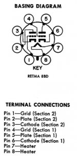
Remember that the tube socket pins are numbered clockwise,
as seen from the bottom of the socket.
Does this apply to all tube/valve pin designations?Remember that the tube socket pins are numbered clockwise,
as seen from the bottom of the socket.
That's different from Solid State Integrated Circuits which show the pin numbers looking down on the top of the socket/IC.
Remember that the tube socket pins are numbered clockwise,
as seen from the bottom of the socket.
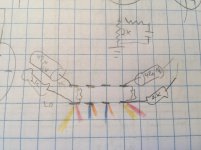
I was using the notch in the center hole of the socket as the starting point to count clockwise from 1 to 8, as explained in pictures like this:
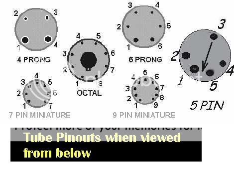
So, in the image I posted before, the 6SN7 pin numbers would use the notch in the center hole as the reference point for locating the space between pins 1 and 8. Here it is (attached) with the pins numbered in yellow. Is this correct?
Attachments

the 6SN7 pin numbers would use the notch in the center hole as the reference point for locating the space between pins 1 and 8. Here it is (attached) with the pins numbered in yellow. Is this correct?
Yes, clockwise as viewed from the bottom.
IC packages use the same convention, clockwise as viewed from the bottom.
That's also counter-clockwise as viewed from the top.
Last edited:
What's tripping me up then is that connection from pin 6 (cathode section 1) to pin 2
(plate section 2). If it's a VA, 6 should be connected to ground, right?
Yes, even if this is a mu follower, the connections are still wrong.
Start another reverse engineering over fresh, maybe you're missing something.
Good advice. When the mind gets stuck on something it can affect perception, so I started from scratch but came up with the same thing.
As I lay awake last night puzzling over this, I remembered that I have a schematic of the Wright WPA 3.5 (6SN7-->2A3) that was reverse engineered by ClefChef (in this post), as well as some of his pics inside the amp. Maybe that could provide some clues about the WLA12.
When I looked at the WPA 3.5 images this morning, low and behold the 6SN7 uses the same topology as the WLA12. I am at work now and will get back to the WLA12 schematic tonight, but at any rate here is ClefChef's schematic and pics of the WPA 3.5 (value of the resistor between caps 2 & 3 in the PS is 2K).
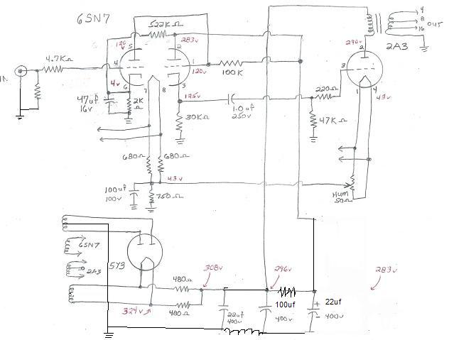
When I looked at the WPA 3.5 images this morning, low and behold the 6SN7 uses
the same topology as the WLA12.
This is the circuit that we expected, with the addition of an extra DC bias loop (522k resistor).
Last edited:
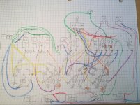
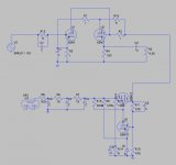
Here is my re-draw of the diagram plus a schematic-in-progress. Unfortunately I couldn't find my colored pencils so I ended up using my kids' cray-pas, which are too thick. Also, some parts of the schematic could use re-organizing but I think it's mostly correct.
It was not possible to read all of the resistor color codes well due to photo quality, so I did my best here.
The WLA12 is a fairly complex circuit, with a high-low gain switch, balance controls, stereo/mono/reverse, source selection, and volume control.
I don't think I did the HV portions correctly in the schematic because I need to meditate for a while on the Hi-Lo switch subcircuit before I understand it.
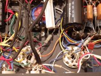
The 6X5 --> 6EM7 heaters are connected in series by the yellow wires. The two 6SN7 heaters are connected in series by the white and blue wires.
The Hi-Lo switch has 8 tabs, in 2 rows of 4.
As you look at the amp from the bottom, the yellow wires from pin 6 (cathode 1) of the 6SN7s attach to the outer tabs of the top (closest) level, while blue wires in the middle of that row attach to a tag strip lug and then a 30K (I think) resistor to pin 1 (grid 2).
Pin 3 (cathode 2) of the 6EM7 attaches by orange wire to a lug on the tag strip, and then to two 2K resistors (one for each channel) that in turn attach a lug, then to pin 2 (plate 2) by orange wire to each of the 6SN7s, which then attach by orange wire to what I think is the central two tabs on the bottom (furthest) row of the Hi-Lo switch. The same lug that feeds pin 2 also attaches to pin 1 (grid 2) by 100K (I think) resistor. Red wires on the bottom outer tabs of that switch go to separate lugs on the tag strip, where it connects by 100K resistors to the lugs that lead to pins 1 and 2. Those lugs also have paralleled resistors (one 22uf 350V and one orange one whose value I can't determine) that apparently go to ground.
I'm still working on all this, but the topology (barring errors) is taking shape.
Not pictured in the schematic are the filament supplies. On the drawing, the HV secondary on the PT connects its center tap to ground. The center tap of the secondary for the 6SN7 filaments connects to a Xicon 10W resistor (value unknown, but it is marked 39J) and one tab of the large 22000uF 25V cap (a blue Sprague) and then the white wires (pink in the drawing) to the 6SN7 heaters (pin 8). The two main wires of that secondary attach to two diodes that go to the other tab on the Sprague cap, and then the blue wire goes to the 6SN7 heater (pin 7).
The Xicon resistor might also connect to ground, but I'm not sure.
Also not pictured on the schematic is what I think to be a 200K resistor that goes from heater to cathode 2 (pins 8 to 3) on the 6EM7. Is that to "lift" the heaters, as people say?
It was not possible to read all of the resistor color codes well due to photo quality, so I did my best here.
The WLA12 is a fairly complex circuit, with a high-low gain switch, balance controls, stereo/mono/reverse, source selection, and volume control.
I don't think I did the HV portions correctly in the schematic because I need to meditate for a while on the Hi-Lo switch subcircuit before I understand it.
The 6X5 --> 6EM7 heaters are connected in series by the yellow wires. The two 6SN7 heaters are connected in series by the white and blue wires.
The Hi-Lo switch has 8 tabs, in 2 rows of 4.
As you look at the amp from the bottom, the yellow wires from pin 6 (cathode 1) of the 6SN7s attach to the outer tabs of the top (closest) level, while blue wires in the middle of that row attach to a tag strip lug and then a 30K (I think) resistor to pin 1 (grid 2).
Pin 3 (cathode 2) of the 6EM7 attaches by orange wire to a lug on the tag strip, and then to two 2K resistors (one for each channel) that in turn attach a lug, then to pin 2 (plate 2) by orange wire to each of the 6SN7s, which then attach by orange wire to what I think is the central two tabs on the bottom (furthest) row of the Hi-Lo switch. The same lug that feeds pin 2 also attaches to pin 1 (grid 2) by 100K (I think) resistor. Red wires on the bottom outer tabs of that switch go to separate lugs on the tag strip, where it connects by 100K resistors to the lugs that lead to pins 1 and 2. Those lugs also have paralleled resistors (one 22uf 350V and one orange one whose value I can't determine) that apparently go to ground.
I'm still working on all this, but the topology (barring errors) is taking shape.
Not pictured in the schematic are the filament supplies. On the drawing, the HV secondary on the PT connects its center tap to ground. The center tap of the secondary for the 6SN7 filaments connects to a Xicon 10W resistor (value unknown, but it is marked 39J) and one tab of the large 22000uF 25V cap (a blue Sprague) and then the white wires (pink in the drawing) to the 6SN7 heaters (pin 8). The two main wires of that secondary attach to two diodes that go to the other tab on the Sprague cap, and then the blue wire goes to the 6SN7 heater (pin 7).
The Xicon resistor might also connect to ground, but I'm not sure.
Also not pictured on the schematic is what I think to be a 200K resistor that goes from heater to cathode 2 (pins 8 to 3) on the 6EM7. Is that to "lift" the heaters, as people say?
Attachments
Last edited:
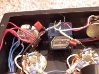
Been doing some more work on this and have gotten further. There are a couple things puzzling me about the 6SN7 section and the Hi/Lo gain switch. You can refer to the wiring drawing in the post above for much of this, as well as the attached pics of what I drew last night.
The hardware used in the amp is a 4PST switch. I've figured out that the low gain mode is in operation when the bottom row of tabs (as seen in pic) is in use, while high gain uses the upper row.
Some observations and questions:
* When in high gain mode, the 100K resistor attached to pin 1 is the sole plate load (for pin 5/plate 1); when in low gain mode, the 30K resistor attached to the blue wire enters in parallel with the 100K, creating an equivalent resistance of 75K and dropping the amount of current and therefore also the gain.
* When in high gain mode, the upper row contains a 47uF 16V cathode bypass cap for 6SN7 cathode one. This in turn connects with a resistor whose value I cannot determine, which then either connects to ground or -- more likely -- to the top of the 2K cathode resistor (see attached drawing). If the unidentified resistor in question goes to ground, then it would exist in parallel with the bypass cap and would simply form a separate cathode assembly from the 2K resistor. However, if it connects to the top of the 2K resistor, then the unidentified resistor would go "across" to the top of the bypass cap, creating a partial cathode bypass situation? Am I way off here?
* The lower (low gain) row contains the 2K cathode resistors (attached to yellow wire) for 6SN7 triode 1, which attaches to a red wire that leads to 100K resistors that in turn feed into the 100K plate load resistors (see yellow circles and lined path in attached pic). I can't imagine why George would add a resistive loop from triode 1 cathode to precede triode 2 Rp. Any ideas?
Thanks,
Jeff
Attachments
...When in high gain mode, the 100K resistor attached to pin 1 is the sole plate load (for pin 5/plate 1); when in low gain mode, the 30K resistor attached to the blue wire enters in parallel with the 100K, creating an equivalent resistance of 75K and dropping the amount of current and therefore also the gain.
100K and 30K in parallel is 23K, not 75K.
That change alone, current will go up, not down.
I'm not clear on the base topology. Some forms seem to have a B+ feed or a plate feed through a large resistor to the cathode. This is a technique to give more bias to the tube without a large cathode resistor; also (if it carries signal) to apply NFB. If this resistor is switched, that also will affect tube current.
adding a 30k in parallel to a 100k gives the combination an effective resistance of ~23k, not 75k...............
Some observations and questions:
* When in high gain mode, the 100K resistor attached to pin 1 is the sole plate load (for pin 5/plate 1); when in low gain mode, the 30K resistor attached to the blue wire enters in parallel with the 100K, creating an equivalent resistance of 75K and dropping the amount of current and therefore also the gain.
That's a massive change.
Maybe you meant a 300k in parallel to the 100k?
adding a 30k in parallel to a 100k gives the combination an effective resistance of ~23k, not 75k.
That's a massive change.
Maybe you meant a 300k in parallel to the 100k?
Ah, I added a 0 when doing the calculation. Oops!
The resistor stripes in question appears to be orange-black-orange (3-0 x1000= 30,000) to me, but I suppose it could be yellow-black-yellow (4-0 x10000) for 400K, which would result in an equivalent resistance of 80K. Or even orange-black-yellow (3-0 x10000) for 300K, but the initial digit and multiplier stripes seem to be the same color to me.
When I get home I'll plot the load lines to gain a sense of what's the most plausible. 23K seems awfully low as a plate load.
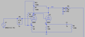
I've been looking at this preamp again and am 95% sure that there's a 100K resistor that comes from 6SN7 cathode 1 and connects to the top of the 100K plate resistor, as in the attached screenshot (cf. R21). Can that be right? I've seen no such technique in the books and online articles I've consulted.
Attachments
- Status
- This old topic is closed. If you want to reopen this topic, contact a moderator using the "Report Post" button.
- Home
- Source & Line
- Analog Line Level
- Wright WLA12 / WLA12A Line Stage Topology