Hello
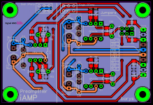
I am currently working on a small OPamp based preamplifier.
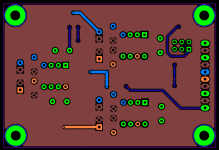
As I have a few single and dual OPamps I would like to make an uniwersal board, so I can select the one of the two section of the PCB.
Setup:
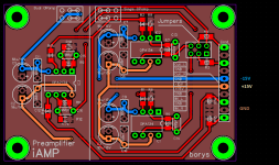
-the preamp board is atatched to the tone controll/volume board
-the RF filter and input capacitor is located just by the 10pin connector header at the mother board.
-on the tone controll board there is capacitor bank for the preamplifier located at the "1st floor''
Now the stuff I do not know which way to go:
1. Do I have to use separate ground return for power section (decoupling) and signal ?
Now the two ground planes (top and bottom) are conneted by the capacitors and 10pin header.
2. Schould I use 10uF MLCC capacitor instead Elko/wima mks2 combo ?
3.Would it be better to use single ground plane (bottom layer) and connect signal return GND with VIAS (instead top ground plane).
4. I have placed 1k resistor just at the OPamp input leg, will I need to add a small cap (RF filter) if the main RF filter is at the mother board ?
5. All the signal traces are 0,5mm width, they will be caring very small current so would it be recommended to reduce trace width to reduce capactive coupling ?
Some questions might be stupid I prefer to ask before Ill will send the PCB for manufacturing.
Best regards
Peter
I am currently working on a small OPamp based preamplifier.
As I have a few single and dual OPamps I would like to make an uniwersal board, so I can select the one of the two section of the PCB.
Setup:
-the preamp board is atatched to the tone controll/volume board
-the RF filter and input capacitor is located just by the 10pin connector header at the mother board.
-on the tone controll board there is capacitor bank for the preamplifier located at the "1st floor''
Now the stuff I do not know which way to go:
1. Do I have to use separate ground return for power section (decoupling) and signal ?
Now the two ground planes (top and bottom) are conneted by the capacitors and 10pin header.
2. Schould I use 10uF MLCC capacitor instead Elko/wima mks2 combo ?
3.Would it be better to use single ground plane (bottom layer) and connect signal return GND with VIAS (instead top ground plane).
4. I have placed 1k resistor just at the OPamp input leg, will I need to add a small cap (RF filter) if the main RF filter is at the mother board ?
5. All the signal traces are 0,5mm width, they will be caring very small current so would it be recommended to reduce trace width to reduce capactive coupling ?
Some questions might be stupid
I prefer to ask before Ill will send the PCB for manufacturing.Best regards
Peter
Attachments
1. Do I have to use separate ground return for power section (decoupling) and signal ?
Do you care about how it sounds or will you be happy with merely excellent measurements? If the latter, then no.
5. All the signal traces are 0,5mm width, they will be caring very small current so would it be recommended to reduce trace width to reduce capactive coupling ?
No, the capacitive coupling will normally be insignificant on a small board such as this. Go thinner and you're more likely to get lifted or broken tracks if and when you come to do mods.
Save
ammel68
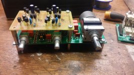
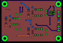
The board with the to92 transistors is a discrete preamp. I need a bit of the flexibility, on the motherboard there is a relay for bypasing the tone controll, output from the board which is ond the top goes straight to the amplifier input. In case I would like to try some new preamplifier I will only prepare a small board and just atatch it to the motherboard.
abraxalito
5. What would you think about two ground planes, the bottom one will cary the power + decoupling and the top one will carry only the signal GND return ?
Would it be correct ?
BIG THANKS
Yeah its a reasonable idea, put the signal GND on the top as that carries almost zero current and join the two together in only one place. However I don't believe that the signal ground plane really needs to be low inductance as generally its feeding relatively high impedance circuits like opamp feedback networks. So star grounding will probably work just as well.
abraxalito
Thanks a lot.
I have splitted the GND's. They are not connected at the preamplifier board. There is star point at the motherboard (bottom one) so all GND is connected at the one point only. I hope it will sound OK.
Regards Peter
Thanks a lot.
I have splitted the GND's. They are not connected at the preamplifier board. There is star point at the motherboard (bottom one) so all GND is connected at the one point only. I hope it will sound OK.
Regards Peter
Attachments
- Status
- This old topic is closed. If you want to reopen this topic, contact a moderator using the "Report Post" button.