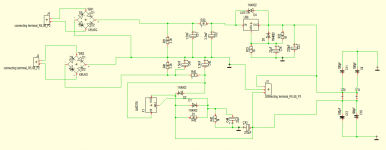
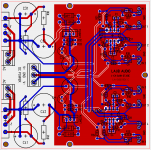
A couple of years back I designed a 4-channel gain stage (line stage) board. Since that time I have revised the design, and I would like to put it out in the public domain for personal (non-commercial) use. The preliminary layout and schematic are attached.
The design includes onboard power supply. In the case that the user already has an appropriate high quality power supply the components in the PS section can be omitted and power supplied to the board via an onboard DC power connector. In the case that the PS section is used, power can be taken from the board from this same connector and used to power other equipment. Note that a dual secondary transformer (not center tapped) or two separate transformers can be used with this design. CRC filtering is used to reduce charging pulses. Regulation is via 317/337 devices with cap stabilized adjust pin.
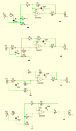
There are four independent gain stages, in pairs, designed around dual op-amps (I show LME49720). The input of each gain stage passes through an RC (EMF) filter and the input ground is lifted via a 4.7R resistor (or similar low value). The lift is used because the inputs are located away from each other and a loop can be formed via the grounds when paths are separated. The resistance should reduce induced currents and, therefore, hum and noise pickup. The amplifier outputs have local HF decoupling and use 68R loading.
I've tried to use sane design and layout concepts. There are multiple star grounds. I am sure that I can still learn a thing or two or three.
Please feel free to comment on this design, point out weaknesses or areas for improvement, etc. I plan to post the production files here after it has had a chance to be vetted.
The design includes onboard power supply. In the case that the user already has an appropriate high quality power supply the components in the PS section can be omitted and power supplied to the board via an onboard DC power connector. In the case that the PS section is used, power can be taken from the board from this same connector and used to power other equipment. Note that a dual secondary transformer (not center tapped) or two separate transformers can be used with this design. CRC filtering is used to reduce charging pulses. Regulation is via 317/337 devices with cap stabilized adjust pin.
There are four independent gain stages, in pairs, designed around dual op-amps (I show LME49720). The input of each gain stage passes through an RC (EMF) filter and the input ground is lifted via a 4.7R resistor (or similar low value). The lift is used because the inputs are located away from each other and a loop can be formed via the grounds when paths are separated. The resistance should reduce induced currents and, therefore, hum and noise pickup. The amplifier outputs have local HF decoupling and use 68R loading.
I've tried to use sane design and layout concepts. There are multiple star grounds. I am sure that I can still learn a thing or two or three.
Please feel free to comment on this design, point out weaknesses or areas for improvement, etc. I plan to post the production files here after it has had a chance to be vetted.
Attachments
Sounds like you're looking for next steps for improvement. I'd suggest greater familiarity with layout parasitics and noise injection mechanisms. Marce posts on this extensively. Tomchr's taming the LM3886 page and related layout posts in the chipamp forum may also be of interest.
On a functional level it may be interesting to look into difference amplifiers and consider lower cutoffs for greater RF/EMI (EMF means something a bit different) rejection. Shifting down a bit in frequency may also be of some interest in the RISO compensation, depending on the desired amount of tolerance for load capacitance.
Probably more current is being pulled from the regulators than is necessary here, though it's not a big deal. Nice job on including protection diodes. But check the polarity of D1 and D2.
Sounds like you're looking for next steps for improvement. I'd suggest greater familiarity with layout parasitics and noise injection mechanisms. Marce posts on this extensively. Tomchr's taming the LM3886 page and related layout posts in the chipamp forum may also be of interest.
On a functional level it may be interesting to look into difference amplifiers and consider lower cutoffs for greater RF/EMI (EMF means something a bit different) rejection. Shifting down a bit in frequency may also be of some interest in the RISO compensation, depending on the desired amount of tolerance for load capacitance.
Probably more current is being pulled from the regulators than is necessary here, though it's not a big deal. Nice job on including protection diodes. But check the polarity of D1 and D2.
Thanks for your comments. I was hoping for slightly more specific feedback... I could pour over tomchr's posts ad nauseum but nothing would dawn on me... I'm too green at layout to even know what I don't know, or where I could improve.
Can someone point out areas that could be improved with a little more detail and specificity?
Also, is the existing design OK for audio, or are there serious flaws?
Thanks.
Can someone point out areas that could be improved with a little more detail and specificity?
This is a 55MHz op amp, so a top layer ground plane is needed, preferably with smt local decoupling caps.
Use the SOIC device package for best results.
Also place C1-C4 as close to the inverting and output pins as possible, and use smt cog/npo types for these.
Last edited:
OKness depends, in general, upon precision targets. If you're good with probably, oh, -80dBish errors and a few dB of CMRR the approach here is fine.
For layout I'd suggest first understanding how copper geometry affects RLCG parameters and after that relating back to circuit performance.
For layout I'd suggest first understanding how copper geometry affects RLCG parameters and after that relating back to circuit performance.
This is a 55MHz op amp, so a top layer ground plane is needed, preferably with smt local decoupling caps.
Use the SOIC device package for best results.
Also place C1-C4 as close to the inverting and output pins as possible, and use smt cog/npo types for these.
Unfortunately only hole components can be used on this project. Is there a better lower GBW op-amp for audio band and gain around 6dB - 12dB?
There are local decoupling C0G caps close to the power pins.
Can you explain why a ground plane is needed if the bandwidth is restricted by the feedback cap? This wouldn't attenuate HF above the audio band? I could move these closer to the device pins (next to them).
Pours aren't necessarily required, though reducing layout inductance is seldom a bad idea. Tim Green's series on op amp stability will help with understanding how the 1/beta intercept moves with GBP and signal gain.
The TI/Burr-Brown OPA 16xx parts are good alternatives to the LME497xx series.
The TI/Burr-Brown OPA 16xx parts are good alternatives to the LME497xx series.
Can you explain why a ground plane is needed if the bandwidth is restricted by the feedback cap?
This wouldn't attenuate HF above the audio band? .
At 55MHz the device/component/pcb parasitics require careful layout.
Even a via can cause problems.
At 55MHz the device/component/pcb parasitics require careful layout.
Even a via can cause problems.
I thought this was only the case if there were 55MHz signals running around the circuit. Is it a good idea to just assume that these will be picked up from ambient RF?
I thought this was only the case if there were 55MHz signals running around the circuit.
Is it a good idea to just assume that these will be picked up from ambient RF?
The op amp can make its own hf from the energy in random noise.
The op amp can make its own hf from the energy in random noise.
Wouldn't that require a high Q resonance or underdamped feedback path in the circuit? Or is that kind of thing more common that one might think?
If I just limit the active devices to slow audio op-amps, can this layout work?
If there is a high quality multi-channel gain stage available, I know some people who want to buy them (or build them). I don't want to push this design on anyone if it has too many flaws.
Wouldn't that require a high Q resonance or underdamped feedback path in the circuit?
If I just limit the active devices to slow audio op-amps, can this layout work?
If there is a high quality multi-channel gain stage available, I know some people who want to buy them (or build them).
At RF you do have resonances in that layout from the parasitics in the pcb and components.
For a commercial product I'd use lower bandwidth devices, since the gain is only 12dB.
Build some prototypes and loan them to interested parties for some field tests.
At RF you do have resonances in that layout from the parasitics in the pcb and components.
For a commercial product I'd use lower bandwidth devices, since the gain is only 12dB.
Build some prototypes and loan them to interested parties for some field tests.
OK. I'm not interested in building anything like this myself. I used to, but gave up for exactly the kind of reasons that we are discussing here. I'm more of a software kind of guy anyway (see signature).
So, if I had to look for a lower GBW active device, thru hole, same DIP-8 package, dual op amp drop in replacement what GBW ceiling should I be staying under? Do any suggestions for op-amps come to mind? OPA2134 for example (8MHz GBW)?
Do any suggestions for op-amps come to mind? OPA2134 for example (8MHz GBW)?
Yes, that one should be ok. Still, it should be built and debugged. This will be a kit?
My original idea was to post the gerber files for anyone to use, build, modify or whatever. The design and layout are derived from one that I built a few of a couple of years back. I never put a scope on them so I can't say what was going on above the audio band. In the audio band there were no problems...Yes, that one should be ok. Still, it should be built and debugged. This will be a kit?
If someone wants to take this concept and run with it to make a "proper" 4-channel gain stage board (onboard PS optional) this is a good thread to do it in! Like I mentioned (I think) in the OP I have been contacted by people who want my original board. I thought I would make a few changes and post the result here for "vetting" in the hopes that it would be improved, but honestly I am no circuit designer and it seems perhaps there needs to be significant changes made, although I would like to hear from some other voices on that. Maybe this should be turned into a group effort for the public domain. But I could not do much more than what you see here on my own.
I'm still looking for more (specific) feedback on design changes that I could make that might improve the layout or circuit.
I will change the op-amp to the OPA2134. I could add a ground plane to the bottom layer if that would help reduce EMF pickup, etc.
Specific advice (e.g. do X at place Y in the layout/circuit, traces at position Z may cause problems so try doing XYZ) is very much more appreciated then, e.g., general advice to go off and read about some aspect of circuit design or layout.
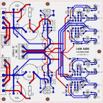
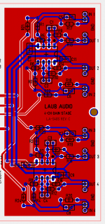
I can easily add a ground plane to the layout, like the attached example (a screen shot of the RH side of the board layout). The ground plane is on the bottom (red) layer, but I could add a top layer ground plane around the traces as well. I still need to move a couple of components around, and the ground plane is done at the end.
NOTE that I just plopped in a ground plane area in the attached example but did not actually connect it to ground anywhere so this is just an example.
Where do I connect the ground plane into the ground system? In between the two PS caps C33 and C43 (the reservoir caps just downstream from the regulators, at center of board)? I assume I do not want the ground plane to be connected into the audio star ground...
Attachments
Where do I connect the ground plane into the ground system? In between the two PS caps C33 and C43
(the reservoir caps just downstream from the regulators, at center of board)? I assume I do not want
the ground plane to be connected into the audio starground...
The entire audio circuit, including decoupling, regulator common, and the final large filter capacitors
should be connected to the ground plane. This replaces the star ground. The remainder of the power supply's
common connection can be at the middle of the left side.Keep the +/- traces above/below this common connection
to minimize loop area.
Many would place the whole power supply on the ground plane. This can work quite well with careful component placement,
when charging currents don't circulate near the audio loops.
Last edited:
The entire audio circuit, including decoupling, regulator common, and the final large filter capacitors
should be connected to the ground plane. This replaces the star ground. The remainder of the power supply's
common connection can be at the middle of the left side.Keep the +/- traces above/below this common connection
to minimize loop area.
Many would place the whole power supply on the ground plane. This can work quite well with careful component placement,
when charging currents don't circulate near the audio loops.
OK, I think I can do something like that. I extended the ground plane area to include the regulator circuit and the final PS caps in the attachment. I would fold all of the ground traces on the bottom layer (red lines with white auras) into the ground plane and move other traces to the top where/when possible. The result would be that everything that goes to ground would connect directly into the ground plane. Is that correct? See attached.
Attachments
result would be that everything that goes to ground would connect directly into the ground plane. Is that correct?
Yes, we want as low impedance ground returns as possible, and the pad on the ground end of a resistor, etc.
should be directly connected to the ground plane, with thermal relief to allow good soldering.
Connect the grounds traces on the top layer to the ground plane also.
Move the feedback caps close to the op amp pins also. Move R1/R5/R13 up a little, and move R9 down a little, to allow this.
Also watch the mounting holes, since the screw heads can short to the ground plane, so allow more clearance.
Last edited:
- Status
- This old topic is closed. If you want to reopen this topic, contact a moderator using the "Report Post" button.
- Home
- Source & Line
- Analog Line Level
- 4-channel gain stage with power supply