Hi,
recently I faced an Offset problem with the Borbely JFET Buffer design.
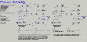
Attached is the dimensioned circuit asc.
IV-converters built around Q1/2/R17/C7 resp. Q3/4/R23/C9 feed over DC-blocking caps C1 resp. C5 into the buffers.
Power supply lines are +-12.7V from a Dual linear reg.
Each supply line supplies two -inverting to each other- IV-converters and buffers.
R5/C2 and R14/C6 modulate the CCS (J2/R4 and J4/R13).
The buffer´s supplies generate from the main supplies over the RC-filters R8/C3 and R9/C4.
R8 and R9 differ by the paralleled resistance of the modulating resistors R5 and R14 which add to R8.
The outputs are grounded through a Relais-contact for one minute.
Now, after the relais release, the output voltages drop instantely to ~-6.5V, as do the gates of all four JFETs.
Well, the Gates of J2 and J4 have to settle close to the negatve supply line, but J1´s and J3s Gates should settle at 0V.
Most circuits remain in this Offset condition.
Only a few eventually (sometimes it takes a couple of minutes) recover and settle within a couple of mV around 0V.
I´ve never had this kind of Prob earlier.
Running from the original non-regulated +-14.7V things worked.
It seems that after adding the Dual LDO that drops the supplies to +-12.7V the problem occured.
Sims show indeed a small ´glitch´ of the gates of J1 and J3 and the outputs into the negative, but in a range of less than -1V and quickly approaching 0V again.
I had Offset probs with this kind of circuit using BF246 JFETs, of which I found out that the BF246 went into Latch-Up (Temperature rise -> Gate Leakage rise -> Id rise -> temperature rise).
But the working conditions for the LSK289C are so different here, that Latch-Up can´t be the mechanism.
Also the JFETs are still fine.
After a Latch-Up they´d be destroyed.
Hard grounding J1´s and J3´s Gates didn´t help either.
As soon as the Gates are released they and the corresponding outputs drop to -6.5V.
I haven´t seen any reports yet about such a prob or a similar one.
Does anybody have a clue what´s going on here?
I´m already close to desperate, especially as a nearly identical circuit works flawlessly.
The similar circuit uses MMBF4391s as cascodes to the LSK389Cs.
Thank You in advance.
jauu
Calvin
recently I faced an Offset problem with the Borbely JFET Buffer design.
Attached is the dimensioned circuit asc.
IV-converters built around Q1/2/R17/C7 resp. Q3/4/R23/C9 feed over DC-blocking caps C1 resp. C5 into the buffers.
Power supply lines are +-12.7V from a Dual linear reg.
Each supply line supplies two -inverting to each other- IV-converters and buffers.
R5/C2 and R14/C6 modulate the CCS (J2/R4 and J4/R13).
The buffer´s supplies generate from the main supplies over the RC-filters R8/C3 and R9/C4.
R8 and R9 differ by the paralleled resistance of the modulating resistors R5 and R14 which add to R8.
The outputs are grounded through a Relais-contact for one minute.
Now, after the relais release, the output voltages drop instantely to ~-6.5V, as do the gates of all four JFETs.
Well, the Gates of J2 and J4 have to settle close to the negatve supply line, but J1´s and J3s Gates should settle at 0V.
Most circuits remain in this Offset condition.
Only a few eventually (sometimes it takes a couple of minutes) recover and settle within a couple of mV around 0V.
I´ve never had this kind of Prob earlier.
Running from the original non-regulated +-14.7V things worked.
It seems that after adding the Dual LDO that drops the supplies to +-12.7V the problem occured.
Sims show indeed a small ´glitch´ of the gates of J1 and J3 and the outputs into the negative, but in a range of less than -1V and quickly approaching 0V again.
I had Offset probs with this kind of circuit using BF246 JFETs, of which I found out that the BF246 went into Latch-Up (Temperature rise -> Gate Leakage rise -> Id rise -> temperature rise).
But the working conditions for the LSK289C are so different here, that Latch-Up can´t be the mechanism.
Also the JFETs are still fine.
After a Latch-Up they´d be destroyed.
Hard grounding J1´s and J3´s Gates didn´t help either.
As soon as the Gates are released they and the corresponding outputs drop to -6.5V.
I haven´t seen any reports yet about such a prob or a similar one.
Does anybody have a clue what´s going on here?
I´m already close to desperate, especially as a nearly identical circuit works flawlessly.
The similar circuit uses MMBF4391s as cascodes to the LSK389Cs.
Thank You in advance.
jauu
Calvin
Attachments
Last edited:
What does C2 do?
The buffer without C2 works perfectly.
The drop across the upper source resistor matches the drop across the lower source resistor.
Dennis Feuch describes this version of the DCB1 in detail (long before the DCB1 was thought of).
His paper is linked on this Forum.
My old link is dead.
Here is a new one
http://www.google.co.uk/url?sa=t&rc...unZLUGcKBXggi7w&bvm=bv.67720277,d.ZGU&cad=rja
How do we get rid of all that google rubbish and generate the direct link?
Last edited:
Hi,
C2 couples the signal dependant voltage drop over R5 to the lower JFETs gate.
This way the CCS is modulated by the audio signal.
The result is not a SE-CCS behaviour but rather a push-pull behaviour.
It reduces output impedance and improves current drive capability.
Its documented in Borbely´s JFET articles.
I shorted R5 and took out C2 and even reduced R6 to 100k to see if it worked, but the Offset remained.
I still have no explanation for the phenomen.
jauu
Calvin
......
Running from the original non-regulated +-14.7V things worked............
oscillations ?
can you up output voltage of regs used in problematic setup , to differentiate is problem in voltage or in regs nature ?
The outputs are grounded through a Relais-contact for one minute.
Now, after the relais release, the output voltages drop instantely to ~-6.5V, as do the gates of all four JFETs.
Calvin
Are you short-circuiting the outputs or are you unloading them?
You could have burned J2 and J4, and when the relay is off only the lower 27ohms load the LDU into it's current limiting.
Can you measure the voltage drop over R3 R4 R5 the 100 ohms and the two 27 ohms?
It would also be interesting to see if this is caused by an interaction between the IV converter and the buffer or if it's just a problem with the buffer. Removing the 470nf coupling cap would separate part of the path and let you see if the buffer by itself is having trouble.
---Gary
---Gary
I have used the Feucht style Buffer and have not seen an offset problem when using the dual polarity supply.
I have also used the Feucht style Buffer on a single polarity with DC blocking caps on both the input and the output, very similar to the original B1. The only difference is the added source resistor fitted to the upper and lower jFETs. Again there is no offset problem. But there is potentially a charge up problem, on start up, to build up the half supply voltage on the output capacitor. I have not experienced this as a problem. I do not hear a click/thump on start up probably due to pre-amp starting up more quickly than a power amp.
I have also used the Feucht style Buffer on a single polarity with DC blocking caps on both the input and the output, very similar to the original B1. The only difference is the added source resistor fitted to the upper and lower jFETs. Again there is no offset problem. But there is potentially a charge up problem, on start up, to build up the half supply voltage on the output capacitor. I have not experienced this as a problem. I do not hear a click/thump on start up probably due to pre-amp starting up more quickly than a power amp.
Calvin,
Some months ago, I tested your buffer and had an issue at start up.
The output sticked always close to the -Ve rail. But removing the cap for push-pull operation and all was fine, nothing destroyed.
I'm using LSK389/4391 in metal casing at +-15V psu and I thought it had to do with the common substrate.
I tried Werner's pcb with single parts and had no problem. The goal was very low and stable offset, hence the dual metal parts.
For me, the cure was a diode across the 1Megohm biasing resistor of the lower jfet.
It clamps the charging pulse to -Ve at start and has very low voltage accross it in opération.
Since, it works...
Regards,
Francis
Attachments
Hi,
thanks so far for Your efforts.
As some of You report, the simple JFET-Buffer is not known to be critical or overly sensitve.
So it came as a surprise to me first time, when the BF246 equipped Buffers failed.
The reason for this were the working conditions which drove the JFETs into Latch-Up.
Unfortunately is Latch-Up seldomly mentioned in literature and hardly ever specced in the DSs.
At first the LSK389C equipped Buffers showed no sign of malfunction until recently.
As I could exclude Latch-Up as the mechanism behind, start-up conditions were the first candidate.
So I shorted the 100R Drain resistor and omitted with the 220nF modulator-cap.
No difference ... still heavy offset.
Next I connected a medium-ohmic resistor - and eventually a dead short- via the relais contact to gnd.
This reduced offset at start-up, but as soon as the relais opened it jumped to -6.5V and remained there.
Next idea was to short the input biasing resistor (220k) to gnd at start-up.
It kept the Gates of J1 and J3 and the outputs closely to 0V.
On relais opening the offset jumped to -6.5V again.
Now it only requires only a small mismatch of 65µA in Idss to generate a -6.5V ofset over the 100k preset loading resistor, but with the matched JFETs in one casing, the Offset should generally be less than 10mV.
Weird thing also, that the LSK389C/MMBF4391 cascoded Buffer stages (even two of them paralleled and modulated) don´t show this effect, but all work flawlessly.
One would expect them to be much more prone to oscillation and misbehaviour than the simple stage.
I haven´t tested the Diode idea yet.
It looks quite promising in the simulation.
While the diode-less output drops into the negative range (-1.2Vpeak), recovering slowly to 0V, the dioded output swings positive (~+2V, depending on Diode) first, quickly approaching 0V with only a minimal and short swing over into the low negative (-20...-160mV).
I´ll try that modification first and report back.
jauu
Calvin
ps: Francis, as You had a similar problem also with the LSK389C (metal TO71 casing, without external substrate pins), I wonder if the substrate pins 3 and 7 of the plastic SOIC casing, which I left nc, required to be grounded? Unfortunately Linear Systems doesn´t specify anything in their rudimentary DS.
Last edited:
Hi,
thought about the possible mechanism(s) for the high offset again and searched the net for clues.
I hold it possible, that a combination of Gate leakage plus impact ionization is responsible for the phenomen.
Both mechanisms could lead to a too high Gate current, that -in combination with the 220k gate resistor- would create a Gate voltage so high and negative in value that the gate, and hence the source, may be driven to this excessive offset value.
Unfortunately most DSs specifyy Igss only for unrealistic conditions of Id=0 and Vds=0, at 25°C.
Igss increases exponentially with temperature, roughly doubling per every 10°C temperature rise.
The DS of Siemens BF246/BF256 shows a Igss over temperature curve with an 100x increase from 25°C to 100°C and nearly 1000x from 25°C to 125°C.
Measured under non-realistic Id=0 and Vds=0 condition.
The DSs of Toshibas 2SK170 and 2SK389 show a diagram of Igsx (gate excess current) over Vds.
I assume this to be a diagram of impact ionization which starts to shoot up at around 1/4 of Vgds (-40V), hence ~10V of Vds.
The diagram also doesn´t account for the temperature related increase of impact ionization.
It also only shows Igsx for a Id range < Idss.
Since the upper -and much more so the lower- JFETs are biased positvely (Vgs>0) drain currents in excess of Idss can flow.
Now the Igss of the SK170 and alike is specced at rather high 1nA.
Considering Vds, Id and temperature in a range where Gate leakage and impact ionization may be in effect, a disastrously high Gate current may apply.
The afore mentioned BF246 for eample specifys a Igss of up to 5nA and lower Vgds (25V).
Failure of both the BF246 and the LSK389 buffers could be explained by these mechanisms.
With the LSK389 buffer it´d need ~30µA of gate current to produce a gate voltage of -6.5V over the 220k Gate resistor.
The simulation doesn´t sim temperature effects nor impact ionization, which explains the lower offset values against the praxis.
Counter measures could be to reduce the Vds (Supply voltages), add more cooling and to keep the Vgs of the JFETs -especially the lower J2 and J4- negative.
The proposed (Schottky) Diode does exactly the latter.
Omitting with the modulating cap also keeps J2/J4´s Vgs negative.
With C2/C6 in place J2/J4 are heavily biased positive.
I hope that the explanation is correct and that the Diode-Tweak will do the job.
I´ll report.
jauu
Calvin
Last edited:
Calvin,
I discover impact ionization...
But I remember having thought I had a thyristor in place of a jfet.
For me, it made the nasty effect disappear.
In your case, not sure a diode will help, it's rather related to high leakage.
Francis
I discover impact ionization...
But I remember having thought I had a thyristor in place of a jfet.
So I shorted the 100R Drain resistor and omitted with the 220nF modulator-cap.
No difference ... still heavy offset.
For me, it made the nasty effect disappear.
In your case, not sure a diode will help, it's rather related to high leakage.
Francis
Hi,
without Diode the lower JFETs undergo quite a long period of positive Biasing (sim says >600mV) with an associated large Id (sim says ~30mA, which would be 50% higher than the specced maximum!).
Indeed became the JFETs hot quite quick, indicating high drain currents.
With the (Schottky-)Diode in place the lower JFETs Vds stays negative and the associated Id sims around 6mA, and so it stays well within safe and sane limits.
Only the upper JFETs may be shortly biased positive, resulting in a short positive output pulse, but quickly approaching 0V after.
Seems that the Diode is a useful if not necessary modification for this kind of Buffer when JFETs are used with highish Gate leakage, high Gate resistor value, and under Vds conditions >1/4 of Vbreakdown, and under high Id and elevated Temperature conditions.
Wonder about no mentioning of that effect for E.Borbelys Buffers and others using 2SK170 or similar JFETs, as there are even higher Vds conditions and at drain currents of Idss.
Maybe its really some weird effect of the common-substrate JFETs?
jauu
Calvin
Last edited:
- Status
- This old topic is closed. If you want to reopen this topic, contact a moderator using the "Report Post" button.
- Home
- Source & Line
- Analog Line Level
- Offset Problem with Borbely JFET-Buffers