I have a phono Section that uses two op27's cascaded. First stage is I to V. Second is a differential stage with most of the riaa.
The op 27 has dc offset nulling. Can I run the first stage with negative bias, and correct the second stage to zero bias thus biasing the second stage into class a?
Or since the second stage is differential, is it not possible? The stage is Peter Daniels.
Thanks!
The op 27 has dc offset nulling. Can I run the first stage with negative bias, and correct the second stage to zero bias thus biasing the second stage into class a?
Or since the second stage is differential, is it not possible? The stage is Peter Daniels.
Thanks!
Last edited:
A phono stage with a current input? Did I miss something?
Anyway, class A biasing is something that's applied to the output stage, usually by sourcing or sinking current into one of the supplies (depending on what's more beneficial). It is most useful when the opamp has copious output current capability but is run at low idle current. Fast but power-efficient types like LM6171, or the trusty MC33178/179. An OP27 is not particularly powerful by today's standards, I wouldn't want to load it with more than 5 mA or so.
Anyway, class A biasing is something that's applied to the output stage, usually by sourcing or sinking current into one of the supplies (depending on what's more beneficial). It is most useful when the opamp has copious output current capability but is run at low idle current. Fast but power-efficient types like LM6171, or the trusty MC33178/179. An OP27 is not particularly powerful by today's standards, I wouldn't want to load it with more than 5 mA or so.
Last edited:
Thanks for your reply!
Nope, you did not miss anything. It's a phono stage with current input dedicated to MC cartridges.
Once the output is biased into class A, a coupling cap becomes necessary correct?
Will using the DC offset nulling features of the chip once again take it out of class A?
Nope, you did not miss anything. It's a phono stage with current input dedicated to MC cartridges.
Once the output is biased into class A, a coupling cap becomes necessary correct?
Will using the DC offset nulling features of the chip once again take it out of class A?
... It could be tricky to implement given the existing board is so very tight.
Not at all. Make a simple, one JFET, 3mA CCS and solder it between opamp's output pin (pin 6 on single opamp chip, pins 1 and 7 in dual opamp chip) and the opamp's negative rail (pin 4 on both versions of opamp case).
Of course, for dual opamp chip you'll need two CCSs per chip.
2sk117 are fine. No series resistor, but you'll need gate resistor and possibly a source resistor to set the Id to about 3mA.I have 2 pieces 2SK117GR.
Does it matter if it is on the output or on the negative input? No series resistor is necessary?
Must check local shop for 2SK246Y.
No input connection is needed, read carefully post #6.
Google for "JFET as constant current source" to understand what are you trying to do - you give a strong impression that you don't.
Be careful !So I bought some 246GR from the local shop.... 60 cents each, all 8 pieces are fake. IDSS is zero.
Same test jig shows that IDSS on the two pieces of 2sk177GR is 3.3 and 4.8..... my K170 show 6.5, 7.3....
Dang!
2sk117 has a different pinout than 2sk246 - DGS vs. SGD. There's a possibility that you connected yours 2sk246 in a wrong way.
Google for datasheets and do you your best to understand them.
You are correct -- I'm new at this and trying to learn as I go along. My avatar/handle refers to my size, not my ability. The subject is quite broad.
I am very appreciative of your help!
Google returns things I am not clear about.... like applying bias voltage at the inverting input of the op amp vs applying bias current at the output.
I will look at the charts to set VGS to obtain the correct Id. At this point the only way I have done that is via LED strings in the Salas DCB1.
Thank you!
Regarding the 246, they are enhancement mode FETS of some sort. When testing with gate tied to drain, and 10 volts applied to source, there is no current flow. When moving the gate to the source, about 8.5 volts flows across the 10 ohm resistor attached from drain to PS return.
Using 2sk246 in enhancement mode (N-channel part with gate more positive than the source) will easily burn them. They are N-channel depletion mode JFETs which means the gate being negative compared to Source (usually gate is at 0V and the source at some positive voltage).
Read this to understand JFETs:
http://linearsystems.com/assets/med... The New Frontier Part 1, by Erno Bordely.pdf
http://linearsystems.com/assets/med... The New Frontier Part 2, by Erno Bordely.pdf
http://linearsystems.com/assets/med...rt 1 to 4, by Ray Martson, Nuts and Volts.pdf
And here is the nice story (especially Method Two) to help you understanding biasing opamps into class A:
Biasing Op-Amps into Class A
Chew through that and you won't wander in the dark anymore...")
Read this to understand JFETs:
http://linearsystems.com/assets/med... The New Frontier Part 1, by Erno Bordely.pdf
http://linearsystems.com/assets/med... The New Frontier Part 2, by Erno Bordely.pdf
http://linearsystems.com/assets/med...rt 1 to 4, by Ray Martson, Nuts and Volts.pdf
And here is the nice story (especially Method Two) to help you understanding biasing opamps into class A:
Biasing Op-Amps into Class A
Chew through that and you won't wander in the dark anymore...
The jFET is built/manufacturered as either depletion or enhancement.
Once made it cannot be changed.
The k246 is an Nchannel depletion mode jFET.
To measure Idss one connects Gate to Source, then applies voltage from Darin to Source.
This ensures that Vgs= zero and when Vds = manufacturer's test voltage (often 10Vds) and Tj = manufacturer's test temperature (usually 25°C) you end up with Idss.
Fortunately most jFETs are manufactured such that they are symmetrical with respect to Drain and Source. They work with Drain and Source swapped.
i.e. connect Gate to Drain and apply voltage from Drain to Source and you can with the correct temperature and the correct voltage get a measurement of Idss.
Provided you have connected the voltage source correctly (an Nchannel must have Source more negative than Drain), doing your drain connected to gate test, may not have blown up the Nchannel depletion mode jFET.
When you connect the gate to the wrong pin (was Drain) and it is now swapped to become a Source, the G+swapped Drain is still connected to the more negative voltage with respect to the swapped Source pin(which is now the Drain).
Get this wrong and you will blow up the jFET.
Last edited:
Thanks for the info Juma, and thank you AndrewT for the details.
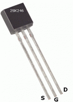
With the flat of the transistor up, I see the pins from Left to Right as S,G,D. I assume that this is drawn showing the pins, and we are looking at the transistor from the bottom, not the top. I used the classicCMP drawing.
Will report once retested.
With the flat of the transistor up, I see the pins from Left to Right as S,G,D. I assume that this is drawn showing the pins, and we are looking at the transistor from the bottom, not the top. I used the classicCMP drawing.
Will report once retested.
Without the photo and schematic it's not totally clear what you really did in that "jumpered to" experiment of yours
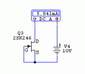
To avoid possible confusion about resistor value, pinout and similar, please find attached clear pic of the 2sk246 pinout and the simplest Idss testing schematic. Just read what the mA-meter says.
To avoid possible confusion about resistor value, pinout and similar, please find attached clear pic of the 2sk246 pinout and the simplest Idss testing schematic. Just read what the mA-meter says.
Attachments
Juma,
Sorry I was not clear.
The photo agrees with my interpretation of the pin out on the data sheet. In the previous test, the 10 ohm resistor was actuall 9.6, so 120 mA was obtained.
Since you were kind enough to supply a drawing, I'll explain how the tests were set up. All "jumpers" are wires with alligator clips at either end. They implement the connections in the drawing.
NEW TEST:
DC source is set to -10V.
DC source (-10V) is connected to Gate and Source. (G+S is clamped by an alligator clip of one jumper, source is clamped by the other alligator clip of the same jumper).
Drain is connected to DMM ma/A input. ( Drain jumpered to DMM mA/A input)
DMM gnd is connected to DC source return (+) ( DMM Gnd jumpered to DC source return (+) ).
Meter set to mA.
Result: 122 mA Idss.
I can upload some photos if that helps.
Sorry for being suspicious but JFET with 120 mA is definitely not a 2sk246. Don't even know what JFET that might be - I used few dozens of different types and never had in my hands a TO-92 JFET with such a high Idss (highest Idss I measured was 2n4391 with 75mA).
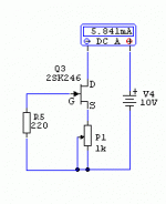
Nevertheless if it's JFET you can use it as a CCS - make a setup as drawn in attached schematic and vary P1 to achieve Id of 3mA, then disconnect it and measure the resistance set with P1 and put in the circuit closest fixed value resistor. If a P1 of 1k doesn't get you to 3mA add more resistance in series with it.
Nevertheless if it's JFET you can use it as a CCS - make a setup as drawn in attached schematic and vary P1 to achieve Id of 3mA, then disconnect it and measure the resistance set with P1 and put in the circuit closest fixed value resistor. If a P1 of 1k doesn't get you to 3mA add more resistance in series with it.
Attachments
- Status
- This old topic is closed. If you want to reopen this topic, contact a moderator using the "Report Post" button.
- Home
- Source & Line
- Analog Line Level
- op amp class a bias