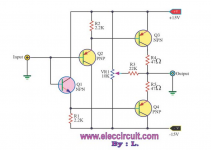
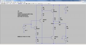
I built the following buffer circuit using BC550B/BC560B devices. After powering the circuit up for about 30 seconds, the transistors are all too hot.
Is this because they aren't biased correctly or am I using the wrong transistors all together?
The circuit doesn't state which devices to use.
Thank you...
Is this because they aren't biased correctly or am I using the wrong transistors all together?
The circuit doesn't state which devices to use.
Thank you...
Attachments
Yes, the emitter should go to the 47 ohm. I wouldn't like to guess how well it will work though, its a bit of an unlikely looking circuit at first glance. Also your transistor/s may have suffered as a result of the problem... just try it though, it will either work or it won't ")
No, Q3 in your drawing is a PNP (Emitter arrow pointing toward the Base), you need a NPN (Emitter arrow pointing away from base), and yes, as the output stage is an emitter follower, the emitter for Q3 should connect to R4. If you have stability (oscillation) problems after you make those changes, try putting a 1 kOhm resistor between the input and the bases of Q1 and Q2.
Mike
Mike
Q3 is shown to be a NPN in the drawing and that's what I used. So, I need to reverse the emitter and collector connections?
Q3 is drawn as an PNP. Q1 is drawn correctly as an NPN. Look at the way the arrow points on the emitter. It points out for an NPN.
Sorry, I wasn't actually looking at the symbol, but at NPN on the diagram.
Ok, I switched the emitter and collector on Q3 and the circuit does work as far as audio going through it.
Problem now is I can't get the DC offset below .170V with adjusting the trimmer. I didn't have a 10K trimmer, so I took a 5K and added 6.8K ohm resistors in series on the end pins connecting to the power supply rails.
No, Q3 in your drawing is a PNP (Emitter arrow pointing toward the Base), you need a NPN (Emitter arrow pointing away from base), and yes, as the output stage is an emitter follower, the emitter for Q3 should connect to R4. If you have stability (oscillation) problems after you make those changes, try putting a 1 kOhm resistor between the input and the bases of Q1 and Q2.
Mike
Thanks Mike for the suggestion. I went ahead and put a 1K ohm resistor in series with Q1 and Q2.
That circuit is just old National Semiconductor LH0002.
http://www.ti.com/lit/an/snoa725a/snoa725a.pdf
http://www.ti.com/lit/an/snoa725a/snoa725a.pdf
Sorry, I wasn't actually looking at the symbol, but at NPN on the diagram.
Ok, I switched the emitter and collector on Q3 and the circuit does work as far as audio going through it.
Problem now is I can't get the DC offset below .170V with adjusting the trimmer. I didn't have a 10K trimmer, so I took a 5K and added 6.8K ohm resistors in series on the end pins connecting to the power supply rails.
You could try reducing the 22k.
(This offset trimmer is one reason I said in my first post that the circuit "looks a bit unlikely". A buffer whose output can be altered by injecting 0.5ma or so into the output... isn't much of a buffer to my way of thinking)
Hi,
the circuit is dimensioned a bit ahm ... unlucky.
The two input transistors (Q1,2) of this Diamond-Buffer are running on ~6.5mA.
This is much more than required and leads to ~100mW of heat power losses in each transistor.
So they will will run quite hot without cooling fins.
The output transistors Q3,4 on the other hand are running on low 1mA bias current.
This limits the useable drive into the load to unnessesarily low <2mA.
Following changes to the circuit improve matters.
Change R1,2 to 4k7 (they are intended as ccs, so higher R-value is better)
Change R4,5 to 22R (lowers output impedance --> better for driving lower impedance loads)
Connect the now unused 47R resistors between the emitter of Q2 and the node R2/Q3 resp. the emitter of Q1 and node R1/Q4 (raising the Ube of the output transistors, hence their bias current)
Change R3 to 10k (improves DC-offset voltage correction range)
These measurements will reduce the bias through Q1,2 to 3mA and reduces the heat power losses to ~50mW each.
It will raise the bias current through R3,4 to 5.5mA allowing more drive into the attached load and lowers the THD considerably.
Q3s and 4s heat power loss will be ~80mW each.
jauu
Calvin
Hello Calvin,
Thank you for analyzing the circuit and all the suggestions!
I noticed that Q1 and Q2 were running noticeably warmer than Q3 and Q4, which I thought was odd and figured it should be just the opposite.
Now Q3 and Q4 are running warmer than Q1 and Q2.
After doing all your modifications, the circuit sounds better and I'm able to adjust the offset to near zero.
Are there any particular transistors that you recommend for Q1-Q4?
I'm currently using N5401 and N5550 for the input transistors and MPSA devices for the output transistors.
Also, how much output current is this design limited to? Would 100mA be possible with the right transistors?
Thanks again...
For interest I simulated this. Its load driving ability is limited as you might expect and distortion increases dramatically if the load is reduced to 100 ohms. This is at 6 vrms into 600 ohm.
I'm not sure what you have done with the 47 ohms.
I'm not sure what you have done with the 47 ohms.
Attachments
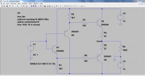
Thank you for the simulation.
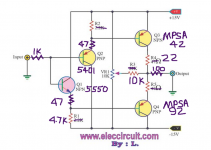
As suggested by Calvin, I put the 49.9 ohm resistors(closest value I have) in series with Q1 and Q2's emitters like I've tried to show in the drawing below.
I have also shown the circuit as I'm using it now.
Hmmm...I see your circuit doesn't contain the 10K ohm trimmer or the 10K ohm resistor in series with the center pin(wiper?).
Are the trimmer and resistor not really needed?
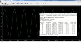
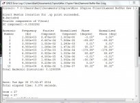
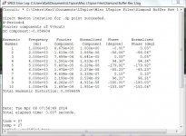
As for the second image you posted, I have to admit that I really don't understand what I'm looking at.
For instance, I have no idea what "Harmonic Number", "Fourier Component", "Normalized Component", or the 2 different Phase columns are showing me.
Distortion at .039% I do understand.
The output sine wave looks like it goes from -8V to +8V. Is that correct?
As suggested by Calvin, I put the 49.9 ohm resistors(closest value I have) in series with Q1 and Q2's emitters like I've tried to show in the drawing below.
I have also shown the circuit as I'm using it now.
Hmmm...I see your circuit doesn't contain the 10K ohm trimmer or the 10K ohm resistor in series with the center pin(wiper?).
Are the trimmer and resistor not really needed?
As for the second image you posted, I have to admit that I really don't understand what I'm looking at.
For instance, I have no idea what "Harmonic Number", "Fourier Component", "Normalized Component", or the 2 different Phase columns are showing me.
Distortion at .039% I do understand.
The output sine wave looks like it goes from -8V to +8V. Is that correct?
Attachments
Last edited:
What load impedance do you want to drive and to what level ? You probably could pull 100ma but I wouldn't think it would be very linear.
I'm looking at being able to drive the input of most power amps(input impedance of most amps I've seen are usually between 20K-50K ohms) with interconnects probably no longer than 2 meters or so.
Thank you for the simulation.
As suggested by Calvin, I put the 49.9 ohm resistors(closest value I have) in series with Q1 and Q2's emitters like I've tried to show in the drawing below.
I have also shown the circuit as I'm using it now.
Thanks... I kept reading what Calvin had written... it was the word "between" that confused (me
)What is surprising in the simulation is just how much those added 47 ohms increase the distortion raising the figure to 0.12%
Hmmm...I see your circuit doesn't contain the 10K ohm trimmer or the 10K ohm resistor in series with the center pin(wiper?).
Are the trimmer and resistor not really needed?
They are needed (or you use some other means) if the DC offset is a problem. In the simulation of your circuit, it needs 3.8k to the +15 rail to trim the offset to zero. Unfortunately that makes the distortion worse again, and by a huge margin as you can see.
As for the second image you posted, I have to admit that I really don't understand what I'm looking at.
For instance, I have no idea what "Harmonic Number", "Fourier Component", "Normalized Component", or the 2 different Phase columns are showing me.
Distortion at .039% I do understand.
The output sine wave looks like it goes from -8V to +8V. Is that correct?
Yes, the voltage is approx. 16 volts peak to peak or 8 volts peak. That becomes slightly less than 6 volts rms (vpk/1.414). I set the input voltage to be 6 volts rms (8.5 volts peak) but the loading on the output pulls the level down. That shows the design has relatively poor drive ability. A good opamp would maintain the level with absolutely no change as it was loaded.
The fourier components show the relative amplitudes of the first 10 harmonics (number one is the base test frequency). They will make more sense as a graph as shown where you can see the amplitudes.
I'm looking at being able to drive the input of most power amps(input impedance of most amps I've seen are usually between 20K-50K ohms) with interconnects probably no longer than 2 meters or so.
That it will do easily
If we increase the load to even 10k the distortion falls dramatically to around 0.008% (I also removed the 3.8k trim because that is also part of the "load" and so increases distortion)
Attachments
the output emitter resistors are shown as 22r.
If we were to apply the usual EF optimal bias voltage the output bias current would be only just over 1mA.
Self and others have confirmed that an EF has less distortion the lower the emitter resistor values.
Would this circuit work with 2r2 instead of 22r?
Adjust to full ClassA bias voltage using say Vre of 50mVre to 100mVre (two to four times optimal ClassAB).
Could you attach the (*.asc)s for the 3 plots shown in post18?
Last edited:
- Status
- This old topic is closed. If you want to reopen this topic, contact a moderator using the "Report Post" button.
- Home
- Source & Line
- Analog Line Level
- Transistors in Buffer Circuit Running Too Hot