Thanks for your input jean-paul, hopefully the design will evolve some in that period!
With regard to the universal control of this board do we think it would be useful to include a level translator on the PCB? The CS3318 needs 3.3V logic control and it's something I've considered already since PICs are typically 5V and even if they're not, a lot of LCDs are so we need level translation somewhere.
Perhaps including a level translator IC on board and extending the input header to include a simple supply voltage input for the controlling board to connect to when desired (between 1.8-5V should then be possible) but also a jumper which can be installed when 3.3V logic is desired anyhow.
It appears that the 74HC4050D is most suitable for the level translation task, it basically permits an over-voltage condition at the input so that 5V (or even higher) logic may be used, as may 3.3V. Compatibility with 2.5V logic isn't unrealistic looking at the typical transition voltages but couldn't be guaranteed. 1.8V logic wouldn't be permissible. Unless anyone knows of a more suitable shifter solution?
For the digital rail watchdog, a TPS3823 appears suitable. The Master Reset can be forwarded on to the control header, via the level shifter, to give conventional functionality. This just provides the guarantee that the device will enter reset when the digital rail is removed (drops below 2.93V).
I think my current de-coupling scheme is as recommended? I have used the 4x100nF parallel with 4x10uF between +V and -V rails shown in the datasheet. I just want to be certain my ground to +/-V de-coupling is also sufficient.
That was a long read! Had seen some of those images around previously but not the whole thread. A lot of work been done by linux-works there, but certainly I now get the feeling that this chip is somewhat finicky 
I quite like the opto-isolator solution to level conversion and perhaps the ACPL-244-500E quad isolator will suit. Does require more current from the microcontroller however and I'm not sure it gives much benefit over the 74HC4050D, is isolating the control electronics fully particularly important? This design appears to use isolation though (Toshiba TLP281-4):
M-81
It sounds like your findings are that removal/failure of the 3.3V line before the analogue while the device is powered is a condition which causes a destructive fault. The TPS3823 watchdog should be able to prevent this but it includes a 200mS delay to reinstating the reset high which might be annoying to have to work around in code. The thread references the demo board but I can't quite figure out how they're handling it on that, I think the biased transistor devices are just to drive the status LEDs?
It sounds like your findings are that removal/failure of the 3.3V line before the analogue while the device is powered is a condition which causes a destructive fault.
I can confirm this, fried two of these ICs already!
Oh dear, and they're not cheap either, especially when mounted on a PCB like this where you're unlikely to remove it without damaging the board too.
We'll need a failsafe way to protect the chip from this condition. Provided the analogue section is fully shut down when the device is reset then it's quite simple, but I might feel safer using analogue regulators with a shutdown feature which is then activated whenever there is no 3.3V present. Will be a bit of a hunt to find those I think, the negative one at least.
maxw, how are you using your ICs now or did you abandon because of their vulnerability?
I think my current de-coupling scheme is as recommended? I have used the 4x100nF parallel with 4x10uF between +V and -V rails shown in the datasheet. I just want to be certain my ground to +/-V de-coupling is also sufficient.
It is. Just checked again.
maxw, how are you using your ICs now or did you abandon because of their vulnerability?
Yeah I abandoned the project after frying the second one. They are not cheap, then you have to pay VAT and postage in the UK.
I'm sure you can think of an elegant simple solution though! Could just have more caps on the 3.3 line so on power down it will be the last to go. Not sure about fail safes though...Many regulators have enable/shutdown features you could use. LT1963A/LT3015 do but the negative reg doesn't come in SOT223 or anything that small which is annoying, only 5-LEAD PLASTIC DD package.
Of course the development board just regulates the 3.3V from the 8-9V input, think it would still be a problem if the -9V remained on though.
I will probably try with the LM2941/LM2991 pair of adjustable regulators. More expensive for sure but if it can save the CS3318 chip unconditionally then it's worth it. It's Ground for ON function too so would need a simple inverter running from the pre-regulator analogue supply to force shutdown. Then again perhaps simply putting the chip into reset state as soon as loss of 3.3V power is detected will suffice.
I will probably try with the LM2941/LM2991 pair of adjustable regulators. More expensive for sure but if it can save the CS3318 chip unconditionally then it's worth it. It's Ground for ON function too so would need a simple inverter running from the pre-regulator analogue supply to force shutdown. Then again perhaps simply putting the chip into reset state as soon as loss of 3.3V power is detected will suffice.
I fried several also. Discovered the problem by disconecting my Lcduino from the testboard. I used the 5V supply from de Lcduino to power the VD with a 3.3V regulator.
This is watchdog chip I used:
Max6301
MAX6301, MAX6302, MAX6303, MAX6304 +5V, Low-Power, P Supervisory Circuits with Adjustable Reset/Watchdog - Overview
This is watchdog chip I used:
Max6301
MAX6301, MAX6302, MAX6303, MAX6304 +5V, Low-Power, P Supervisory Circuits with Adjustable Reset/Watchdog - Overview
Discovered the problem by disconecting my Lcduino from the testboard. I used the 5V supply from de Lcduino to power the VD with a 3.3V regulator.
But this would be fine if the Reset was also disconnected (and had a pull-down resistor) since the device would enter low-power mode and shut down even its analogue circuits? I guess the issue arises when Reset is held high by an external supply and the local 3.3V is removed.
Was your main reason for choosing that Maxim IC that you could disable the timer? That's the only thing putting me off of the TI device (which is quite a bit cheaper) is that when we write code, we must wait 200mS from removing Reset to the chip actually becoming addressable, to account for the delay through the watchdog. Not too big an issue since code is so easily modified though. Basically all we really need is a comparator set to trigger around 3V and an AND gate so we can still operate the Reset function as we wish most of the time, but the TI watchdog offers this functionality through its MR (Master Reset) input pin, provided the delay isn't an issue.
The implementation with shutdown regulators isn't as practical as I thought. It is fairly easily done on the positive regulator, using the pre-regulator voltage, low side MOSFET switch and zener to produce a shutdown signal when the MOSFET is turned off. However, the negative regulator also requires a positive logic signal and so we couldn't guarantee the device in the event that both positive analogue and 3.3V rails are lost as there would be no source for the logic shutdown control. Only way round is feedback to the microcontroller which can perform the shutdown, relies on the user code to protect the device though, or using a small DC-DC to produce the positive logic from the negative pre-regulator input. Too many obscure peripheral parts needed now!
I chose this one because it is highly configurable and Farnell stock them.
According the datasheet the chip has to be kept in reset until the digital supply is stable. The burning problem only occurs after the registers are written and Powerdown bit is set. If you remove the VD in this state it goes wrong.... But luckily the analog part powers down immediately if a reset is given.
According the datasheet the chip has to be kept in reset until the digital supply is stable. The burning problem only occurs after the registers are written and Powerdown bit is set. If you remove the VD in this state it goes wrong.... But luckily the analog part powers down immediately if a reset is given.
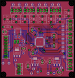
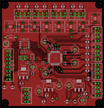
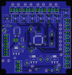
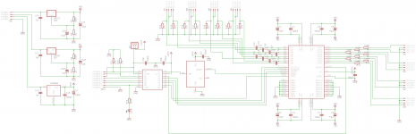
Hey all, here is revision 2! This now has:
The possible limitation is lack of I2C control, since the pull-up resistors can't be used with this level converter, unless it is acceptable to place them between the converter and the CS3318? I was certainly planning to use SPI myself, I can't imagine being too concerned with requiring an extra microcontroller I/O pin in DIY applications. I've only seen discrete MOSFET solutions to I2C level conversion and that makes for a whole lot of part placement+soldering when 6 channels of data are involved.
Any feedback appreciated!
- Molex 4-pin input and output headers (stereo with dual ground). A good combination of flexibility and sturdiness (the 2-pin type are a bit flimsy) I hope.
- Level conversion from 5V to 3.3V, or can be unused by placing the jumper (for direct 3.3V control). Additionally, the ENout pin now forwards to the header at whatever interface voltage is being used. An LED also shows when the chip is out of reset condition.
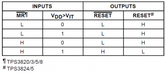
- A watchdog IC ensures the device is held in reset if the digital supply falls below 3V. Observe the truth table; the 3.3V power must be present and stable and !MR must be high for the device to come out of reset:
- Discharge resistors on the inputs to eliminate connection/disconnect pops.
- Reset and Mute are connected with pull-down resistors at the control header, as advised the Mute should be else if it is not connected back at the microprocessor it can cause issues, and for Reset this ensures the default condition is to be in reset.
The possible limitation is lack of I2C control, since the pull-up resistors can't be used with this level converter, unless it is acceptable to place them between the converter and the CS3318? I was certainly planning to use SPI myself, I can't imagine being too concerned with requiring an extra microcontroller I/O pin in DIY applications. I've only seen discrete MOSFET solutions to I2C level conversion and that makes for a whole lot of part placement+soldering when 6 channels of data are involved.
Any feedback appreciated!
Attachments
Hi, I am planning a revision to this board utilising more of what I've learned from my recent DAC designs, namely trying to provide a more solid ground return and I may also wish to leave space for larger coupling capacitors. This may be a while coming since I am more busy now with other stuff but if I get the board manufactured there will be 3 produced, so I will likely be selling off 2 ")
- Status
- This old topic is closed. If you want to reopen this topic, contact a moderator using the "Report Post" button.
- Home
- Source & Line
- Analog Line Level
- CS3318 PCB Layout