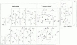
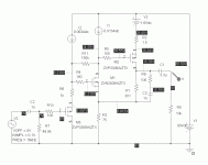
Attached is the schematic for the current implementation of an All-In One solution for MM phono and various inputs on one PCB with common shunt regulator for both channels. The line amp section has gain, so it might serve for folks who have lower gain power amp solutions similar to the SIT amp "L'Amp" or simulated SIT solutions such as "L'Fake Lite". This is a complete preamp on a board, no joke. Later on will be a setup for solutions more comfortable with a unity gain line amp - not a really big stretch.
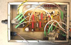
This the the preface to a series of RIAA/line amp solutions that will be checked out in a no-frills test box.
This the the preface to a series of RIAA/line amp solutions that will be checked out in a no-frills test box.
Attachments
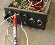
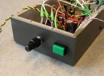
Here is a rear view of the test chassis. The phono input and line outputs get the standard RCA jacks. The source selector has been omitted, and source switching is accomplished via the pigtail RCA jacks at the rear of the chassis. Keep in mind that this is a bare-bones test setup that can be easilly and rapidly swapped in to test a given preamp circuit. I only anticipate switching between a turnatble and a high quality CD player for listening tests, hence the ultimate bare-bones approach to source switching.
Attachments
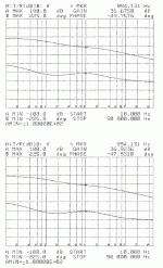
Here is the G-P response of the line amp section . Gain is ~4.8X, and is flat out past 1MHz. Some compensation will be needed to fix the peaking at ~15MHz. It appears that a simple pole will not suffice. More on that later when I can get the pole-zero tweaked to satisfaction.
BTW, on both sets of graphs, the top trace is gain, and the bottom is phase.
BTW, on both sets of graphs, the top trace is gain, and the bottom is phase.
Attachments
I'm reading if nobody else is. In the stock box I have j111 for n channel jfets and 2n7000 for n channel mosfets, but that p channel mosfet in the output would cost me $8 minimum shipping plus whatever it costs. As all my power amps have a lot of gain to cope with a PAS2 output (12AX7), I might just delete that stage. The only problem might be the capacitance of the 6' coax RCA cable.
What C1 & R1 are you using? For what cartridge? My op amp disco mixer uses .033 uf on the input op amp feedback, if that means anything (hums a bit is why I'm thinking of an upgrade). Is C2 your RIAA roll-off capacitor?
Flat past 1 mhz may be a bit of a problem. I do have CB'er driving by. I managed to silence his continuously beeping "Dixie" with a steel box, chokes on the DC power supply inputs to the box, and 100 pf caps to ground on the mag phono inputs.
Last edited:
I am not happy with the line amp section of the preamp, for what turns out to be well-founded (and fundamental) reasons. The problem got uncovered when I started trying to unsnarl the high frequency peaking in the gain-phase plots - more on this when tiime permits. It looks like there's also a solution, though with more parts, I'm afraid...
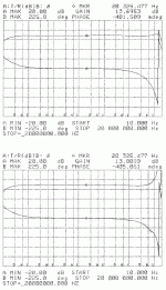
OK, the line amp is flawed. In short, the input is connected right to a gain summing node at the gate of Q7A and Q7B. It's a fairly crude summing node/virtual ground, as the gain around Q7 is low (compared to an op amp), even with the current source loading presented by Q6A/B. In short, the open loop gain/bandwidth of the preamp will depend on the source impedance driving into the Q7 gate. I got an indication of this early on, as the first gain/phase plots I made of the line amp were with the input pots adjusted short of full. With the high driving impedance represented by the input pot at less than full tilt, the gain-phase plots showed none of the high frequency peaking evidenced by the plots shown here. Subsequent measurements were done with the pots turned up to 100%.
The gain-phase analyzer has an intermediate source impedance (600 ohms?), and causes problems at high frequency. Driving the inputs with the 50 ohm impedance square wave output of a function generator gave me 50 ns edges on the output waveform, with no evidence of peaking or other antisocial behavior.
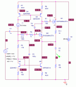
Clearly, you can't have a line amp that that is so heavily dependent on the driving impedance. The circuit attached here isolates the summing nude and fixes the problem (in simulation), at the cost of some more parts. I'll be checking out the real deal as soon as I have time to rig the extra components on my current revision board.
The gain-phase analyzer has an intermediate source impedance (600 ohms?), and causes problems at high frequency. Driving the inputs with the 50 ohm impedance square wave output of a function generator gave me 50 ns edges on the output waveform, with no evidence of peaking or other antisocial behavior.
Clearly, you can't have a line amp that that is so heavily dependent on the driving impedance. The circuit attached here isolates the summing nude and fixes the problem (in simulation), at the cost of some more parts. I'll be checking out the real deal as soon as I have time to rig the extra components on my current revision board.
Attachments
Other folks (SY in particular) have pointed out that with the output of most signal sources, a line amp with gain is usually not necessary. Possible exceptions might designs such as the SIT and "Fake SIT" SE amp designs posted elsewhere on DIYA, and some of the less sensitive Pass amps. I'm trying my hand at several line amp w/gain designs, as it's a nice option to have in one's back pocket, and getting a good clean gain of 5-10X without resorting to something that looks rather suspiciously like an op amp is a challenge.
Having said that, I may settle down to a unity gain line amp, and the circuit shown here is a possibility. Some compensation was needed, as the circuit oscillated like an SOB without it in initial simulation. Distortion as simulated is hilariously low (0.00007%). When it gets down that low, I tend not to quite trust either the simulated THD or harmonic distribution. At any rate, I used some current mirrors to cut down the number of expensive depletion mode mosfets to just one (which would go in place of the current source I used in the simulation). There are jfets that would also work, though with lower output impedance. Using the current mirror also allowed me to remove a level shifting LED from the source of the P-channel mosfet.
At any rate, food for thought for now, as I want to get the stuff I have working before I try something else.
Attachments
A hypothetical amplifier with a gain of 28times producing a maximum output signal of 28Vac (100W into 8ohms and/or 200W into 4ohms) needs 1Vac as Maximum input signal.
An F5 with a gain of 6times produces a maximum output signal of 14.1Vac and needs 2.4Vac as a Maximum input signal.
Both these amplifiers will work well with very many sources if a gain block with switchable gains of +0dB (buffer), or +6dB (2times pre-amp), or +12dB (4times preamp).
The F5 & +12dB requires a Maximum signal of 600mVac
Are there many/any Sources that an F5 would need 10times gain (+20dB) giving a sensitivity of 240mVac to get up to clipping level?
Conventional wisdom has it that non digital source inputs output 150mV and power amps need 1V to drive them to full power.
So, attenuate you CD by 20 dB before it goes into the line stage
Set you line stage gain to 16 dB
and there you have it - the standard hi-fi signal chain gain structure
So, attenuate you CD by 20 dB before it goes into the line stage
Set you line stage gain to 16 dB
and there you have it - the standard hi-fi signal chain gain structure
Are there any or many that are that low?Conventional wisdom has it that non digital source inputs output 150mV and power amps need 1V to drive them to full power.
..................
If there are some and one wants to cater for them, then add a gain stage for that Source ONLY.
Do not attenuate all the other Sources down to this lowest level and then boost them back up to the sensitivity level required by the next stage of amplification.
This is quite the normal way of doing things Andrew. And I works well noise wise.
I have looked at switching the gain on the line stage on the low level inputs, but, for 2V digital source signals, you still have to attenuate by 6 dB to get to the 1 V for the amp input sensitivity. If you are aiming for a nominal 10k input impedance, you are left with 2.5k source, vs attenuation at c. 900 ohms. The other option is to buffer the digital source and then divide down with low value resistors. Works well, but there's added complexity and it is thus inelegant.
I have looked at switching the gain on the line stage on the low level inputs, but, for 2V digital source signals, you still have to attenuate by 6 dB to get to the 1 V for the amp input sensitivity. If you are aiming for a nominal 10k input impedance, you are left with 2.5k source, vs attenuation at c. 900 ohms. The other option is to buffer the digital source and then divide down with low value resistors. Works well, but there's added complexity and it is thus inelegant.
Last edited:
You guys can argue as you like, it's not going to affect what I do. This is a description of a minimal setup with std PCB size to test gain blocks in my system as I devise them, not design-to-order.
So, no switchable gain, no MC input. I have absolutely no incentive to do either.
So, no switchable gain, no MC input. I have absolutely no incentive to do either.
Hi,
I'm working along the same lines as you are.
How would your design compare to a simpler circuit around the LND150? I'm thinking plain common source direct coupled to a source follower with LND150 CCS in the source circuit. All biased 8-12ma. That would be 3 LND150s and 4 resistors plus output cap with high value resistor to ground.
If a non inverting design is required a grounded grid stage direct coupled to the source follower...
I would use a different part than the LND for a current source. The on-resistance on those parts is pretty high, and the current capability rather low for my tastes. I generally use the DN2530N3 or N5 unless I want >100mA, in which case I use an IXYS part.
A simple current-source loaded follower will work OK, though the transconductance will be lower and the distortion somewhat higher. The purpose of the extra parts in my circuit is to get higher transconductance/lower output impedance by means of a short and direct feedback loop. One could also run a mosfet or a darlington at a high bias current to get higher transconductance/lower output impedance, at the cost of more power dissipation.
A simple current-source loaded follower will work OK, though the transconductance will be lower and the distortion somewhat higher. The purpose of the extra parts in my circuit is to get higher transconductance/lower output impedance by means of a short and direct feedback loop. One could also run a mosfet or a darlington at a high bias current to get higher transconductance/lower output impedance, at the cost of more power dissipation.
- Status
- This old topic is closed. If you want to reopen this topic, contact a moderator using the "Report Post" button.
- Home
- Source & Line
- Analog Line Level
- All-In-One Preamp Circuit