PCB design is a very time consuming process to get right. Normally I would say audio doesn't need a ground plane... but don't let me put you off ")
When you actually see the board for real (print it out to scale), what looked like enourmous and wide traces will look very thin. The same goes for the component pads. Make them as big as is feasable.
Are you getting the boards made or diy-ing it all ?
When you actually see the board for real (print it out to scale), what looked like enourmous and wide traces will look very thin. The same goes for the component pads. Make them as big as is feasable.
Are you getting the boards made or diy-ing it all ?
Thanx everyone,
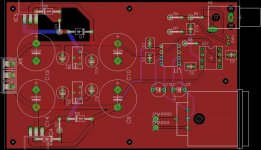
guess I'll be tweaking it for a while still... Here's another update with GND plane, hope its more readable now.
I will be working on it a bit every day, staring at those traces and the schematic.
After a design rule check:
dimension, e.g. parts not lining up to grid points
overlap, looks like i have some tracks on tracks/pads, etc...
drill size issues
After an ERS check:
Power pin IC1 V+ conected to +15V
Power pin IC1 V- conected to -15V
Power pin UI -V0 conected to N$4
Power pin U1 V+ conected to +15V
Power pin U1 V- conected to -15V
Part FRAME1 has no value
Part X4 has no value
Only thing above which may be an issue is the -V0 to N$4 as far as i can tell.
Part X4 is the input power terminal strip.
Cheers,
Chris
Attachments
Yet another layout version
Thanx peranders,
those prev. versions were def. junk! Thanx for the pointers!
The diodes in this next version should block vin from being connected to vout.
Gonna also fix those traces where the parts go through the middle of them!
Cheers,
Chris
Thanx peranders,
those prev. versions were def. junk! Thanx for the pointers!
The diodes in this next version should block vin from being connected to vout.
Gonna also fix those traces where the parts go through the middle of them!
Cheers,
Chris
Attachments
This thread is funny in that I just completed the same design - almost.
The only real difference is that I did not require an input cap for my application, but I can easily wire one from the input connector to the PCB if needed. My input impedance is 470KΩ.
The board sits in a metal box and has two XLR connector pigtails exiting the box and two RCA jacks mounted to the box.
The power supply is a simple wall wart that produces ±15VDC and I added additional filtering inside the box.
Here is the ground plane layer:
I put it into service yesterday and it seems to work fine.
I had 3 PC boards made at ExpressPCB for about $80.
The only real difference is that I did not require an input cap for my application, but I can easily wire one from the input connector to the PCB if needed. My input impedance is 470KΩ.
The board sits in a metal box and has two XLR connector pigtails exiting the box and two RCA jacks mounted to the box.
The power supply is a simple wall wart that produces ±15VDC and I added additional filtering inside the box.
An externally hosted image should be here but it was not working when we last tested it.
An externally hosted image should be here but it was not working when we last tested it.
Here is the ground plane layer:
An externally hosted image should be here but it was not working when we last tested it.
I put it into service yesterday and it seems to work fine.
I had 3 PC boards made at ExpressPCB for about $80.
Last edited:
Hi Loren42,
that is def. hilarious, your design is very much like mine!
I like it, esp. your layout is quite minimalistic! I hope my turns out as nice as yours.
I see your using the 2134 too, a bit more compact for stereo apps. I plan to make five of these for a surround system and put them into a single box.
I've never attempted to make a circuit board before, so its been quite an adventure. I'm using Eagle to do it and I have to say the program is quite good. You seem to have only one ground plane at the bottom. I just want to make a two layer board so my signals will be mixed or "filled-in" with the ground plane polygon. Still have to add one to the bottom layer.
I'm still trying to improve things a bit. It will a little scary to send it off not being 100% sure that its correct. I'm pretty much relying on eagle to check the design and the great people here who know so much more about this stuff than I do.
Say hi to the gators,
Chris
Some Eagle Errors
Hi,
I got these dimension errors in eagle. My RCA jack is violating some minimal spacing distance between the ground plane and its connector....
Not sure how to fix it, since the part itself defines the spacing of its terminals??
Maybe I'll have to find a different brand to use.
Cheers,
Chris
Hi,
I got these dimension errors in eagle. My RCA jack is violating some minimal spacing distance between the ground plane and its connector....
Not sure how to fix it, since the part itself defines the spacing of its terminals??
Maybe I'll have to find a different brand to use.
Cheers,
Chris
Attachments
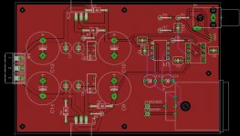
Almost done....
Hi everyone,
I'm getting close to finishing up the layout. Now all of my dimension errors are gone. I replaced the RCA jack with another one to accomplish that.
I also added a ground polygon to the bottom layer, which only has a few signal traces.
I made the traces to the op amp and driver stuff a little thicker but retained most of the thin ones for their pin connections.
The thicks traces are 0.066 and thin ones are 0.032. There's still quite a bit of room to increase them on the regulator side of the board, any suggestions?
Cheers,
Chris
Attachments
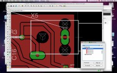
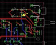
Hi Everyone,
I'm getting to the point were my board layout is just about finished.
My question is:
Do I require a via where the yellow arrow is pointing or is "eagle" smart enough to put one in?
Logically, I would think so, since the capacitors terminal should be connected to both traces.
Would appreciate any comments on that.
P.S. the red lines are on the top layer and blue ones are on the bottom.
Cheers,
Chris
Attachments
Hi Everyone,
I'm getting to the point were my board layout is just about finished.
My question is:
Do I require a via where the yellow arrow is pointing or is "eagle" smart enough to put one in?
Logically, I would think so, since the capacitors terminal should be connected to both traces.
Would appreciate any comments on that.
P.S. the red lines are on the top layer and blue ones are on the bottom.
Cheers,
Chris
It should be automagic.
Worse case is you may need to solder both sides, but generally, al boards have plated through holes.
Thanx guys for your suggestions, ;-)
A couple of other points I've been thinking of...
1. should i add an adj. gain, e.g. a small pot for an additional +6db gain to the buffer?
2. do you guys use sockets for the chips, or do you solder them directly to the board?
I don't think I will req. additional gain, but it would be relatively easy to add?
Typically I'm a KISS kind of a guy, only add what u need however it would possibly
make the board a bit more generic.
Cheers,
Chris
Thanx guys for your suggestions, ;-)
A couple of other points I've been thinking of...
1. should i add an adj. gain, e.g. a small pot for an additional +6db gain to the buffer?
2. do you guys use sockets for the chips, or do you solder them directly to the board?
I don't think I will req. additional gain, but it would be relatively easy to add?
Typically I'm a KISS kind of a guy, only add what u need however it would possibly
make the board a bit more generic.
Cheers,
Chris
KISS says solder in the chips and do not use a variable resistor.
Trimpots are notoriously fragile components and a source for noise. Use them only when absolutely necessary. Removing and replacing a through hole resistor is pretty easy if gain proves to be inadequate. Or, put a trimpot in temporarily and set the gain, pull the pot - measure it - and replace with a fixed resistor.
I would solder my chips because sockets are another weak link that requires a good gas-tight fit between component lead surface and the socket. If that gets compromised, oxidation on the metal will reduce the electrical contact between chip lead and socket.
I also would solder my chips because I have the equipment to remove through hole and surface mount components.
Lastly, you need to consider how often you will be replacing the chip. Chances are it will be never, so sockets just add cost and a small reliability liability that you do not need to carry.
I am not a believer in rolling chips, so I would design it for the intended chips and be done with it.
That is just my opinion. Your needs and feelings may be different.
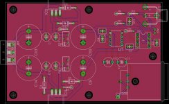
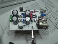
Hi everyone,
I think I have my board layout nearly complete, so I will soon be having the boards made.
Here's a mockup pic of how they will look.
Cheers,
Chris
Nicely done.
Hi,
another question for the experts here.
My main signal traces or better the majority of them are on the top surface where the components are located. My bottom layer has only a few, maybe 5 signal traces.
What do u-all think, should i swap them, e.g. put the majority of the traces on the bottom side?
Does this have any advantages, e.g. like less interfernce with the components?
If that's the case, is there an easy way to swap them with eagle w/o having lay them out again on the bottom layer?
Thanx Again,
Chris
- Status
- This old topic is closed. If you want to reopen this topic, contact a moderator using the "Report Post" button.
- Home
- Source & Line
- Analog Line Level
- Balanced Line Driver with DRV134